 中文
 English

IRF7663 P-Channel MOSFET Replacement: Check the Gate Drive First
 Back to previous page

The IRF7663 is a single P-channel MOSFET in the Micro8 package: 3.05 mm wide, under 1.1 mm tall, -20V, -8.2A, 20 milliohms at 4.5V gate drive and 40 milliohms at 2.5V gate drive, with a gate limit of plus or minus 12V. It sits in the battery master switch of single-cell products, in load switches behind USB ports and peripheral rails, in 5V rail disconnects, and in the transfer between a battery and an adapter. Current in these positions runs from 2A to 6A, the gate rarely moves, and the decision comes down to conduction drop and heat.
The manufacturer now lists the part as obsolete, and distributor stock has gone to zero. The plain IRF7663 code is leaded and fails RoHS; the lead-free order code is IRF7663TRPBF. Projects still carrying this part number are looking at a requalification, not a restock.
VBA8338 fits the footprint: also an eight-pin 3x3 mm part, -30V, plus or minus 20V gate, 18 milliohms at 10V drive and 25 milliohms at 4.5V drive. It does not win at the 4.5V drive point this part was built for, and it has no data at 2.5V. The answer has to be split by gate drive.
Where the part sits
| Position | How it is wired | What it has to do |
|---|---|---|
| Battery master switch | Source to system, drain to pack, gate pulled to ground through a resistor | Conducts all the time, so drop goes straight into runtime |
| USB load switch | Source to load, gate pulled low by a control pin | Survives plug-in surge, static drop feeds the load |
| 5V rail disconnect | In series with the rail, gate on a logic level | Stays low resistance at low gate voltage |
| Battery and adapter transfer | Two devices sharing a drain, gates cross-controlled | Thresholds must match, body diode must not conduct backwards |
What these positions share is a gate that does not move, which makes switching loss irrelevant. That sets the comparison: on-resistance, current rating, and thermal path. Gate charge only matters if the position switches at PWM rates or if standby current is measured in microamps.
The package is Micro8, 3.05 mm wide and under 1.1 mm tall. The same 3x3 eight-pin land pattern also takes MSOP8, and the pinout is identical, which is what makes a swap physically possible.
Breakdown, gate and current limits
Breakdown at -20V: sufficient for a single cell or a 5V rail. A 12V adapter plugged into an unclamped input will ring past that line, and those designs should use a -30V part.
Gate limit at plus or minus 12V: the easiest limit to miss. A P-channel high-side switch turns on by pulling the gate below the source, so with a 12V source the gate sits at -12V, exactly at the datasheet limit, before any ringing. Drive amplitude above 10V, or a source tied to a 12V rail, needs this checked first.
Current at -8.2A: that figure comes from a 25C ambient, a 1.8W dissipation ceiling and a one-inch-square copper pad. On a real board it is not -8.2A. At 70C ambient the datasheet gives -6.6A.
Breakdown and gate voltage are hard limits where an excursion means failure. Current is a soft limit where an excursion means heat. Check the hard ones before discussing conduction loss.
| Parameter | IRF7663 | VBA8338 | Datasheet condition |
|---|---|---|---|
| Package | Micro8 (3.05 mm) | MSOP8 (3x3 mm) | both eight-pin |
| VDSS | -20V | -30V | — |
| VGS max | plus/minus 12V | plus/minus 20V | — |
| VGS(th) | -0.60V to -1.2V | -1.7V typical | ID = -250uA |
| RDS(on) at -4.5V | 20 milliohm max (ID = -7.0A) | 25 milliohm max (ID = -5.6A) | pulse test |
| RDS(on) at -2.5V | 40 milliohm max (ID = -5.1A) | not specified | pulse test |
| RDS(on) at -10V | not specified | 18 milliohm max (ID = -7.0A) | pulse test |
| ID at TA = 25C | -8.2A | -6.0A | one-inch pad, t up to 10 s |
| ID at TA = 70C | -6.6A | -4.6A | same |
| PD at TA = 25C | 1.8W | 2.5W | same |
| Qg | 30nC typical, 45nC max | 16nC typical | ID = -6A, VDS = -10V |
| Ciss | 2520pF | 1600pF | VDS = -10V, 1MHz |
| RthJA | 70 C/W | 40 typical, 50 max (t up to 10 s) | one-inch pad |
| RthJA, steady state | not specified | 95 C/W | — |
| Body diode IS | -1.8A (no temperature basis stated) | -2.1A (board) / -3.5A (case) | Replacement higher |
At 4.5V gate drive
Both parts have data at this point, and both figures are maximums. The original is 20 milliohms, the replacement 25, so the replacement is 25 percent higher.
Carried to actual current:
| Standing current | Original loss | Replacement loss | Difference |
|---|---|---|---|
| 2A | 0.08W | 0.10W | +20mW |
| 3A | 0.18W | 0.225W | +45mW |
| 5A | 0.50W | 0.625W | +125mW |
| 6A | 0.72W | 0.90W | +180mW |
Converting to temperature rise runs into different thermal references. The original has one figure, 70 C/W, measured on a one-inch pad for 10 seconds or less. The replacement gives 40 typical and 50 maximum on the same basis, plus 95 C/W steady state.
At 3A on the short-pulse basis: 0.18W times 70 gives 12.6C for the original, 0.225W times 50 gives 11.3C for the replacement. Roughly even. On the steady-state basis the replacement gives 0.225W times 95, or 21.4C, and the original has no equivalent figure, so 70 is an optimistic stand-in.
At 6A on the steady-state basis: 0.9W times 95 gives 85.5C of rise, which puts the junction at 155C in a 70C ambient, past the 150C limit. The original is rated -6.6A at 70C ambient, so that position is inside its own envelope.
At 2.5V logic-level drive
This is the point the part was designed for. The threshold is specified from -0.60V to -1.2V, so a 2.5V logic pin pulled straight to the gate gives more than 1.3V of overdrive, which is why the datasheet can quote 40 milliohms at that drive level.
The replacement has nothing comparable. The VBA8338 datasheet stops at -4.5V for on-resistance, and its threshold is -1.7V typical, leaving 0.8V of overdrive at 2.5V drive. The channel is not fully enhanced, so its resistance at that point is not 25 milliohms but something much larger, and the datasheet does not give the curve. It cannot be estimated from the 4.5V figure.
The conclusion is narrow: a design that drives the gate directly from 2.5V cannot use this replacement.
Current rating and thermal path
-8.2A and -6.0A were not measured on the same board. The IRF7663 pairs a 1.8W ceiling with 70 C/W. The VBA8338 pairs 2.5W with 95 C/W steady state. Normalised to an 85C ambient, the allowable dissipation is 0.93W and 1.30W, which works out to 6.8A and 7.2A respectively, the latter capped by the 6A package rating.
That arithmetic is worked through in the six-part single P-channel comparison, so this article only takes the result: a 27 percent gap in the headline current becomes 12 percent once both devices sit on the same thermal path, and the direction reverses.
What it means here is that 8.2A and 6A are not comparable as printed. Put both on the same junction-to-ambient resistance, then ask what each can carry at the real ambient of the product.
Gate charge and body diode
Gate charge falls from 30nC to 16nC typical, and input capacitance from 2520pF to 1600pF. Both favour the replacement.
Static switch: the gate moves a few times a day, so neither figure produces loss and neither advantage is realised.
PWM switch: drive loss is charge times amplitude times frequency. At 4.5V drive and 100 kHz with a 2A load, the saved drive loss is about 6mW while the added conduction loss is 45mW. The replacement still loses.
Body diode: the original's -1.8A carries no temperature basis in its datasheet; the replacement is -2.1A at 25C board and -3.5A at 25C case, both above -1.8A, 17% higher on the board basis and double on the case basis. For battery-to-adapter transfer that needs reverse freewheeling, the replacement has more margin, but neither part is meant to work through its body diode, so this sits low in the ranking.
Which cases can swap
| Case | Verdict | Basis |
|---|---|---|
| 2.5V logic pin driving the gate | No | no 2.5V data, threshold does not match |
| 4.5V drive, 2A or less | Yes | 20mW difference, rise is about even |
| 4.5V drive, 3A to 5A | Marginal | 45 to 125mW more, higher steady-state rise, copper must be reworked |
| 4.5V drive, 6A and above | No | 85C rise at steady state, over the limit at 70C ambient |
| 10V drive | Not enough data | original has no 10V figure, 18 milliohms is not a proven win |
| Gate overshoot above 12V | Replacement is better | plus/minus 20V against plus/minus 12V |
| Reverse freewheeling needed | Replacement is better | body diode -2.1A against -1.8A, both board basis |
Set against the rest of the family, the 90 milliohm part IRF7606TRPBF cuts resistance by 80 percent, and the 26 milliohm IRF7726TRPBF is a straight upgrade. The IRF7663 is the only one in this group where the original wins at 4.5V drive, and the reason is simple: it was built for 2.5V and 4.5V logic-level drive, with a larger die than its siblings.
Two other parts in the same footprint
What sets this part apart is that it is the only one in the group with 2.5V data. If the board drives the gate at 4.5V or above, two other parts fit the same land pattern, at the cost of current capability:
| Part | RDS(on) at 4.5V drive | Current class | Fits |
|---|---|---|---|
| IRF7663 (this part) | 20 milliohm | -8.2A, -6.6A at 70C | above 5A, or 2.5V direct drive |
| IRF7726TRPBF | 40 milliohm | -7.0A | 3A to 6A, prefer 10V drive |
| IRF7606TRPBF | 150 milliohm | -3.6A | up to 3A, disconnect only |
At 4.5V drive the order is current first, resistance second. Above 6A this part is the only one left inside its own rating. Around 3A with a 10V drive available, the 26 milliohm part is the upgrade. At 2A or less for pure disconnect duty, the 90 milliohm part cuts resistance by 80 percent and only gives up a current class.
Put another way, the replacement question for this device is not which part to pick, but whether the position still needs 8A. If it does, stay inside the original spec. If it does not, everything gets easier.
Checklist
Gate drive voltage. 2.5V direct drive rules the replacement out. At 4.5V, check the current. At 10V and above, there is no datasheet data and the board has to be measured.
Highest source potential. With the source on a 12V rail, the turn-off gate voltage sits right at the plus or minus 12V limit, and the replacement's 20V rating is the safer choice.
Standing current and maximum ambient. Above 6A at 70C ambient, the replacement exceeds its steady-state thermal path.
Copper area. Both datasheets measure on a one-inch pad. Less copper means higher resistance to ambient, and the replacement's 95 C/W steady state wants more of it.
Reflow profile. A lead-free order code or the replacement requires a lead-free profile, peaking near 260C.
N-channel parts in the same footprint. P-channel and N-channel 3x3 eight-pin parts share a land pattern, so assembly will not catch a wrong reel. Power-up will.
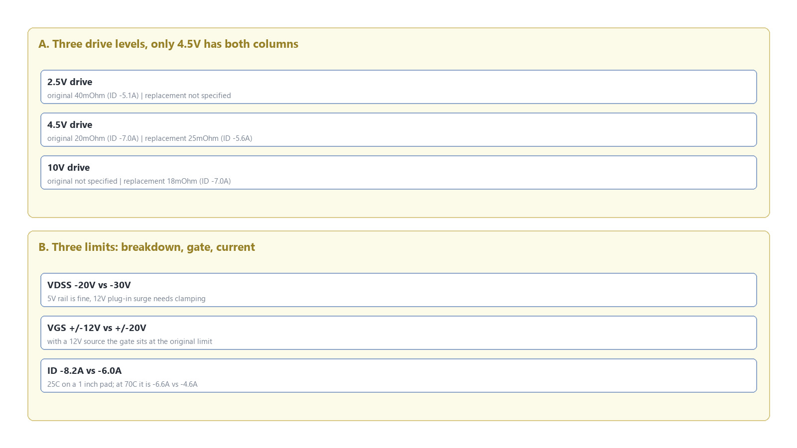
Figure 1. On-resistance of the IRF7663 and the VBA8338 at three gate drive levels. The 2.5V column only has data for the original and the 10V column only for the replacement; 4.5V is the one point where both are specified, at 20 and 25 milliohms.
FAQ
Is the IRF7663 still available? The manufacturer lists it as obsolete and distributor stock has gone to zero. What remains is inventory and reel ends, with mixed date codes and a price premium. Long-term supply means moving to a part still in production.
What is the difference between IRF7663 and IRF7663TRPBF? The same die with a different pin plating: IRF7663 is tin-lead and fails RoHS, IRF7663TRPBF is lead-free. Electrical specifications match at -20V, -8.2A and 20 milliohms at 4.5V drive.
Does the swap to VBA8338 help or hurt at 4.5V drive? It hurts. The original is 20 milliohms and the replacement 25, both as maximums, so the replacement is 25 percent higher. At 3A that is 45mW more, with a similar short-pulse rise and a higher steady-state rise.
Why can the replacement's 10V figure not be used directly? The original datasheet specifies on-resistance only at 2.5V and 4.5V. Extrapolating from 20 milliohms at 4.5V, the 10V value would be lower still, so 18 milliohms is not a proven win. There is no datasheet support for that column, only measurement.
Can a 2.5V logic pin drive the replacement directly? No. The original threshold is -0.60V to -1.2V, which gives enough overdrive at 2.5V. The replacement is -1.7V typical, leaving 0.8V, and it has no on-resistance specification at that drive level.
Does the swap require a PCB change? No. Both are eight-pin 3x3 mm parts with the same pinout. What needs review is gate drive amplitude, copper area and the reflow profile.

Download PDF document
 Download now


