 中文
 English

P-Channel Micro8 MOSFET Selection: 8.2A Rated, 6.8A Usable at 85C
 Back to previous page

Six single P-channel devices in the 8-pad Micro8 / MSOP-8 outline make up this replacement list — four of them out of production, two still shipping — and a -30V part with 18 mΩ at -10V gate drive and a ±20V gate (VBA8338) covers all six mechanically. What the list does not support is a simple "lower resistance wins" story. The highest current rating on it, 8.2A, belongs to a part that can only carry 6.8A on a real board at 85°C ambient, while the replacement's 6A rating survives the same derating. This is written for battery switches, load switches and low-side or high-side P-channel paths that carry under 7A on rails of 24V or less, where the installed part is a single P-channel in a 3×3 mm eight-pad outline. Above 7A, on a rail above 30V, or where the gate hangs directly on a 2.7V or 3.3V logic pin with no driver, neither the outline nor the threshold of the replacement has enough margin.
At a glance
Four of the six originals are gone as catalogue items. IRF7606 is listed as discontinued by Infineon, and IRF7663, NTTS2P02R2 and NTTS2P03R2 are all marked obsolete. The remaining two, IRF7726 and ZXM64P02XTA, are still active — so this is not a supply emergency, it is a decision.
Current ratings across the six are not comparable as printed. They are measured on different board areas with different junction-to-ambient paths, and the spread runs from 70 K/W to 210 K/W. IRF7663's 8.2A and VBA8338's 6A converge to 6.8A and 7.2A once both are referred to the same 85°C ambient.
Gate ratings cluster at ±8V and ±12V for the two 20V ON Semiconductor and Diodes parts, and at ±20V for the three 30V Infineon and ON Semiconductor parts. A ±20V replacement adds headroom to every one of them; it does not license a higher drive amplitude.
Two of the six are still in production
The list is worth reading by column rather than by row. Four parts are dead: IRF7606 discontinued at Infineon, IRF7663 and both NTTS2P02R2 / NTTS2P03R2 obsolete at their makers. Two are alive: IRF7726 at 26 mΩ, and ZXM64P02XTA at 90 mΩ with 6.9 nC of gate charge.
That split changes what the article is for. On a dead part the only question is whether the replacement is electrically safe. On a live part the question is whether the swap is worth doing at all, and the answer differs between the two survivors.
Against IRF7726 the case is clean. Both are -30V, both are ±20V gate, both are -7A class. The replacement drops on-resistance from 26 mΩ to 18 mΩ at the same 10V drive, drops input capacitance from 2204 pF to 1.6 nF, and roughly halves the thermal path, from 70 K/W to a 50 K/W maximum. Nothing gets worse. This is a straight upgrade, not a rescue.
Against ZXM64P02XTA the case is narrower. That part is a -20V device with 90 mΩ and only 6.9 nC of gate charge, and its threshold is specified at 0.7V. It was chosen for a reason that has nothing to do with conduction loss: it is a small, cheap, easily driven switch for a light load. A 3.3V logic pin drives it into full enhancement with 2.6V of overdrive. The same pin against the replacement's -1.76V threshold leaves 1.54V, which is not enough to reach 18 mΩ — expect two to three times that figure, so 36 to 54 mΩ, before temperature. Still better than 90 mΩ, but the margin is not the 5× the headline suggests.
Rated 8.2A, usable 6.8A
This is the part of the list that misleads most reliably. IRF7663 is rated -8.2A, the highest on the list, and it is a 20 mΩ part at 4.5V drive — better than the replacement's 25 mΩ at the same gate voltage. Read only those two rows and the substitution looks like a downgrade on both counts, from 8.2A to 6A and from 20 mΩ to 25 mΩ.
The numbers are not measured the same way. IRF7663 quotes 8.2A at 25°C ambient with a 1.8W dissipation limit, which at a 150°C junction implies a path near 70 K/W. VBA8338 quotes -6.0A at 25°C ambient on a 1×1 inch board, and its datasheet gives a 50 K/W maximum junction-to-ambient for a 10-second pulse and 40 K/W typical. Refer both to an 85°C ambient and the ordering reverses in practical terms:
| Part | Rated ID at 25°C (Ta) | RDS(on) at 4.5V | Path used | Budget at 85°C | Current at 85°C |
|---|---|---|---|---|---|
| IRF7663 | -8.2A | 20 mΩ | 70 K/W | 0.93W | 6.8A |
| VBA8338 | -6.0A | 25 mΩ | 50 K/W | 1.30W | 7.2A, capped by the 6A package rating |
The 8.2A figure is real, but it is a 25°C figure on a board that holds the junction near ambient. Put the same die in an enclosure at 85°C and its usable current is 6.8A — lower than the part it was supposed to outclass. The 27% gap in the ratings is a 12% gap in practice, in the opposite direction from what the datasheet column suggests.
The general rule this produces: a current rating without a thermal path is a number about the test board, not about the device. Before comparing two parts on rated current, put both on the same junction-to-ambient figure and ask what each can carry at the ambient the product actually sees.
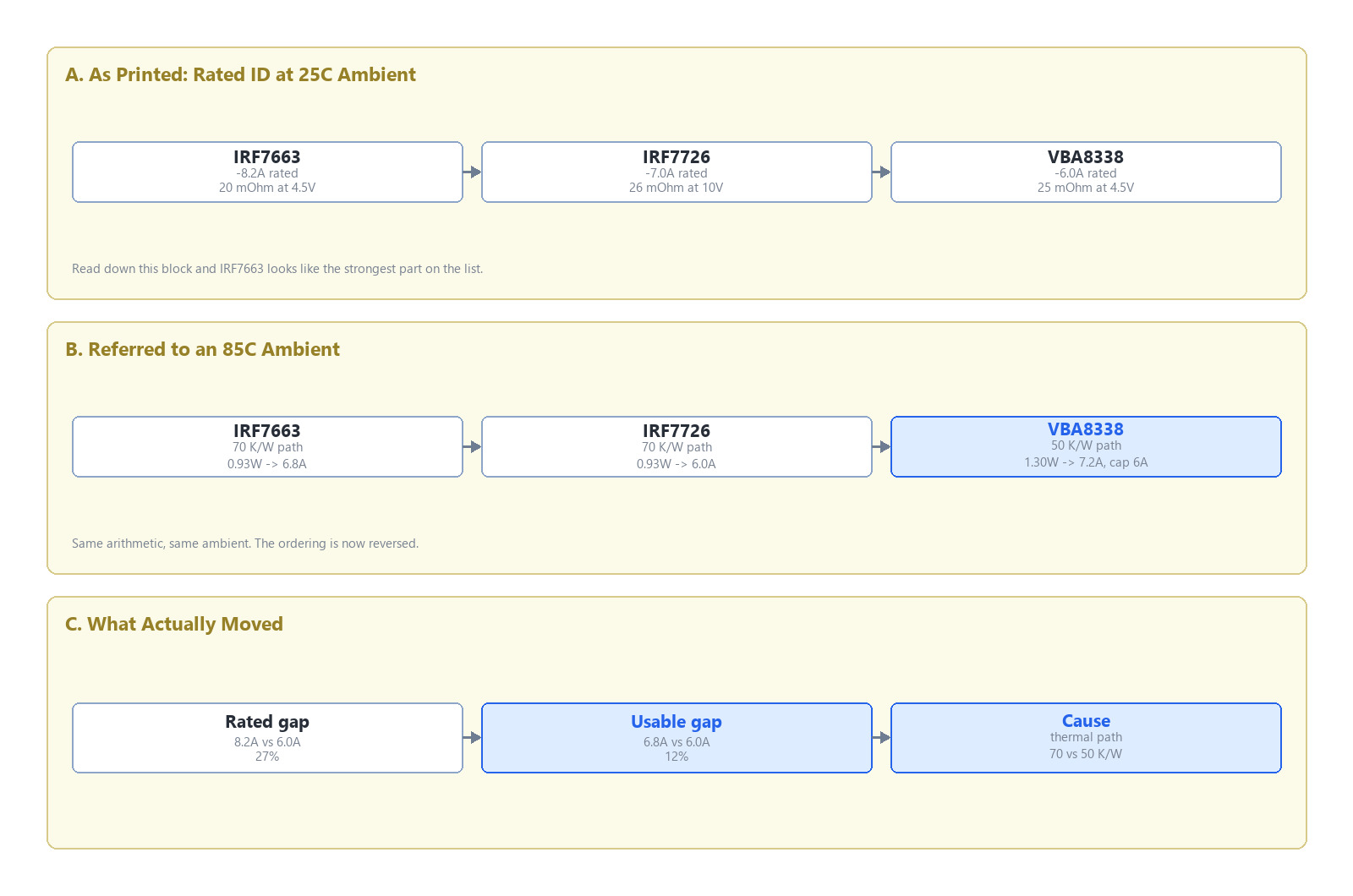
Figure 1. Rated current at 25°C against usable current at 85°C for the six originals and the replacement. The two bars that move the most are the ones whose datasheets quote the smallest thermal path.
The thermal path spread is 5×
The junction-to-ambient figures on this list run from 70 K/W to 210 K/W, in packages that share a land pattern. That is a five-fold difference in how much heat the same copper can move, and it decides the usable current of every part on the list before on-resistance gets a vote.
NTTS2P03R2 is the extreme case. Its datasheet gives 210 K/W on a minimum FR-4 board, 100 K/W on a 2-inch square board, and 0.6W to 1.25W of dissipation depending on which one is used. At its rated -2.1A and 85 mΩ that is 0.375W. On the minimum board the rise is 79°C, so at 85°C ambient the junction sits at 164°C — past the 150°C limit, on a part running exactly at its nameplate current. On the 2-inch board the same current gives a 37°C rise and a comfortable 122°C junction.
Two conclusions follow. First, a 2.1A rating that fails at 85°C on a small board is not a 2.1A part; it is a 1.9A part on that board, and the datasheet note is the only place that says so. Second, any comparison that ignores which board a rating came from is comparing test fixtures.
NTTS2P02R2 has the same shape of problem from the other direction. Its thermal path is 160 K/W and its dissipation is 0.78W — but it is a 90 mΩ part at only -2.4A, so its own conduction loss at rated current is 0.52W and the rise is 83°C. It is a mild, slow, low-current switch that was never meant to run warm.
Against that background the replacement's 50 K/W maximum is the single most useful number on its datasheet. At 3A it dissipates 162 mW and rises 8°C; IRF7726 at the same current dissipates 234 mW and rises 16°C. The copper that was sized to keep the original alive is now doing nothing, which is the good outcome.
Where 78% more gate charge stops mattering
The one figure that moves in the wrong direction against ZXM64P02XTA is capacitance. 900 pF of input capacitance and 6.9 nC of gate charge become 1.6 nF and roughly 12 nC — a 78% increase in the charge the driver has to move every cycle. On a converter that switches at a few hundred kilohertz and idles at tens of milliamps, that is the number that decides efficiency, not on-resistance.
It is also easy to check whether it applies. Gate drive loss is charge times drive amplitude times frequency, and conduction loss is current squared times the resistance difference. Setting the two equal gives the load current below which the extra charge costs more than the saved resistance:
| Switching frequency | Extra gate drive loss | Crossover current |
|---|---|---|
| 20 kHz | 0.48 mW | 0.09A |
| 100 kHz | 2.4 mW | 0.19A |
| 300 kHz | 7.3 mW | 0.33A |
Below those currents the swap costs a fraction of a milliwatt. Above them the conduction saving dominates quickly, and by 1A the saving is around 65 mW against a few milliwatts of extra drive. So the charge increase is not a reason to refuse the substitution at any load that a load switch or battery path would recognise as a load. It is a reason to check one specific case: a part that spends most of its life at under 200 mA with a high switching frequency, where ZXM64P02XTA's low charge is genuinely the reason it was picked.
The threshold matters more than the charge in the same comparison. ZXM64P02XTA specifies 0.7V; the replacement specifies -1.76V. On a 2.7V logic pin that is 2.0V of overdrive becoming 0.94V, and a trench die at under 1V of overdrive is not at 25 mΩ — it is somewhere in the linear region, dissipating more than the part it replaced. Any design that drives the gate from a 2.5V or 2.7V rail directly, with no driver, is the one case in this list where the substitution should be refused rather than recalculated.
The 20V parts are not the same risk as the 30V parts
Three of the six originals are -20V devices: IRF7663, NTTS2P02R2 and ZXM64P02XTA. Three are -30V. Moving all six to a -30V replacement looks like a uniform safety improvement, and for rail margin it is — a 20V part on a 12V rail has 8V of headroom, and any load dump or back-EMF event eats into that directly.
But the gate ratings do not follow the same split. The two lowest gate ratings on the list belong to a -20V part and to a -20V part: NTTS2P02R2 at ±8V and ZXM64P02XTA at ±12V. IRF7663, also -20V, is ±12V. The 30V parts are all ±20V. So polarity of risk is inverted from what the voltage column suggests: the parts with the least rail headroom are also the parts with the least gate headroom, and they are the ones most likely to have had a zener or a clamp added to the gate loop.
That clamp does not come out. A ±8V part that has run for years inside a shipped product is a measurement: the gate node never exceeded 8V, ringing included. Replacing it with ±20V removes the diagnostic and adds nothing to the edge rate, the dv/dt, or the false turn-on margin — those are set by the gate resistor and the pull-down, which were never sized for voltage. If someone raises the drive amplitude because the new part can take it, switching loss, EMI and the body diode's reverse recovery all change at once, with nothing on the datasheet warning about it.
Raising the voltage class is safe. Raising the drive amplitude is not, and they are easy to confuse because both look like using the new part's headroom.
Parameter comparison
| Part | VDSS | ID at 25°C | RDS(on) 10V | RDS(on) 4.5V | VGS max | Vth | Ciss | RthJA | Pd | Status |
|---|---|---|---|---|---|---|---|---|---|---|
| IRF7606 | -30V | -3.6A | 90 mΩ | 150 mΩ | ±20V | -1V min | 520 pF | 70 K/W | 1.8W | Discontinued |
| IRF7726 | -30V | -7.0A | 26 mΩ | 40 mΩ | ±20V | -1.75V | 2204 pF | 70 K/W | 1.79W | Active |
| IRF7663 | -20V | -8.2A | — | 20 mΩ | ±12V | -1.2V max | 2520 pF | 70 K/W | 1.8W | Obsolete |
| NTTS2P02R2 | -20V | -2.4A | — | 90 mΩ | ±8V | -1.4V max | 550 pF | 160 K/W | 0.78W | Obsolete |
| NTTS2P03R2 | -30V | -2.1A | 85 mΩ | — | ±20V | -3.0V max | 500 pF | 210 K/W | 0.6W | Obsolete |
| ZXM64P02XTA | -20V | -3.5A | — | 90 mΩ | ±12V | 0.7V min | 900 pF | 113 K/W | 1.1W | Active |
| VBA8338 | -30V | -6.0A | 18 mΩ | 25 mΩ | ±20V | -1.76V | 1.6 nF | 50 K/W | 2.5W | Active |
Two rows in that table move in the wrong direction and deserve to be named. IRF7663 is the better conductor at 4.5V drive — 20 mΩ against 25 mΩ — and it is gone, so the small loss has to be accepted and paid for in copper. ZXM64P02XTA has less than half the input capacitance, and it is still in production, so the swap is a choice rather than a necessity.
The Vth column is where the two 20V survivors differ most and where the least attention usually goes. ZXM64P02XTA at 0.7V and NTTS2P02R2 at -1.4V maximum bracket a factor of two; the replacement at -1.76V sits outside both. On 4.5V or 5V drive the difference is an overdrive of 3.8V or 2.7V against 2.7V or 2.2V, which is workable. On 2.7V drive it is 2.0V against 0.94V, which is not.
Where this replacement stops working
Three conditions close it out. A rail above 30V needs a different voltage class and a different outline. More than 7A continuous puts an eight-pad 3×3 mm package into a thermal argument it loses regardless of on-resistance, and a SO-8 or DFN with an exposed pad is the honest answer. And a gate driven directly from a 2.5V or 2.7V logic rail, switching at kilohertz rates with no driver — there the -1.76V threshold spends the drive in the linear region, and a 40 mΩ effective resistance at 1A wastes more than the original 90 mΩ part ever did.
The complementary N+P version of this exercise — three parts, all out of production — is worked through in the earlier note on complementary pairs.
One more case belongs here even though it is not electrical. If the BOM carries a P-channel and an N-channel in the same eight-pad outline — common on boards that have both a low-side switch and a high-side disconnect — the two must not share a feeder or a reorder code. The land patterns are identical and the assembly will pass. The failure appears at first power-up, and it looks like a short rather than a wrong part.
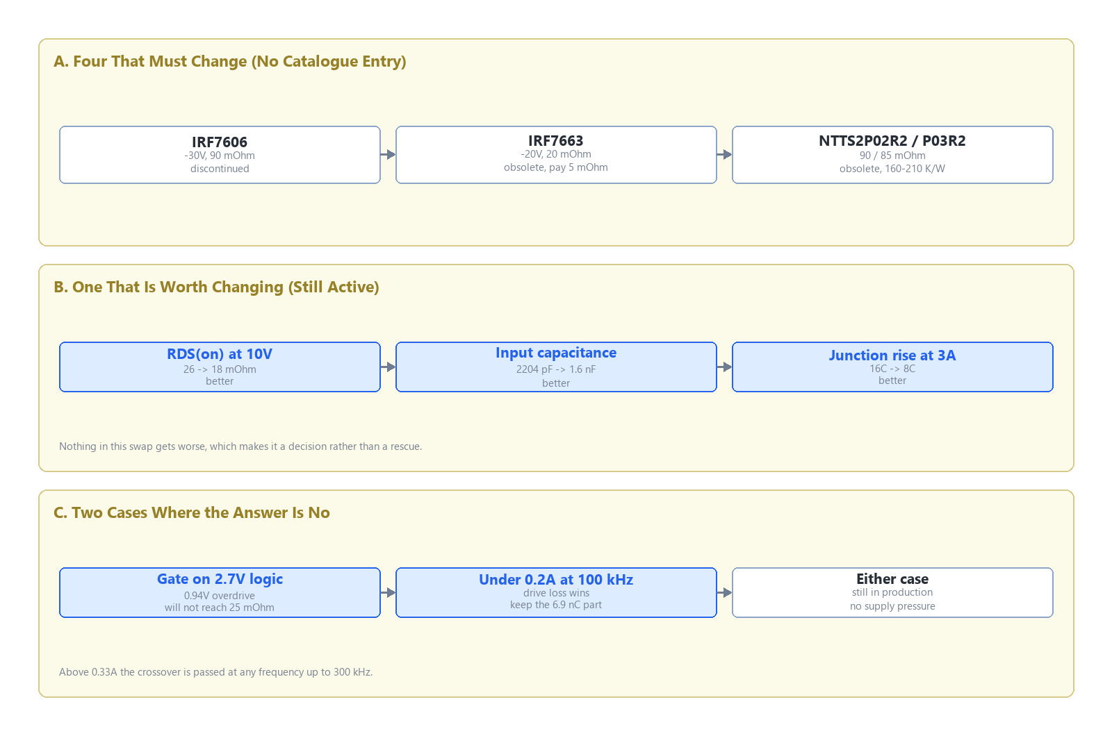
Figure 2. The six originals sorted by what to do with them. The two rows in the bottom block are the only cases where the answer is to leave the installed part alone.
FAQ
Can VBA8338 replace IRF7663 even though the current rating drops from 8.2A to 6A?
Yes, and the drop is largely a change of measurement basis. IRF7663's 8.2A is quoted at 25°C ambient on a 1.8W dissipation limit, implying roughly 70 K/W. VBA8338 quotes 6A at 25°C with a 50 K/W maximum path. Referred to an 85°C ambient, IRF7663 can carry 6.8A and VBA8338 7.2A, capped by its 6A package rating. On-resistance is the real loss: 20 mΩ against 25 mΩ at 4.5V drive.
Is the substitution worth doing when IRF7726 is still in production?
Yes, and that is the cleanest case on the list. Both are -30V and ±20V gate at -7A class, but the replacement has 18 mΩ against 26 mΩ at 10V drive, 1.6 nF against 2204 pF of input capacitance, and a 50 K/W maximum path against 70 K/W. At 3A the junction rise falls from 16°C to 8°C. Nothing in the swap gets worse.
ZXM64P02XTA has only 6.9 nC of gate charge. Does 12 nC break a high-frequency design?
Only below about 0.19A of load current at 100 kHz, where the extra drive loss is around 2.4 mW and the conduction saving has not yet caught up. Above 0.33A the conduction saving dominates even at 300 kHz. The figure to check first is the threshold, not the charge: ZXM64P02XTA at 0.7V works on a 2.7V logic pin, and the replacement at -1.76V does not.
Three of these originals are 20V parts and three are 30V. Is a 30V replacement safe for all of them?
For rail margin, yes — every 20V original gains headroom. What does not transfer is the gate loop. The two lowest gate ratings on the list, ±8V and ±12V, belong to 20V parts, which means those boards probably carry a gate clamp that was added because of the low rating. Keep the clamp and the series resistor exactly as they are; the ±20V rating removes a constraint, it does not remove the reason the constraint existed.
The package and pinout are identical, so what can go wrong?
Polarity of the neighbouring part. An N-channel device in the same eight-pad outline — VBA6317 is the one in this family — shares the land pattern and the pad numbering, so a feeder or reorder mistake between a P-channel and an N-channel part passes assembly and fails at power-up. Match polarity, not just footprint.

Download PDF document
 Download now


