 中文
 English

Complementary MOSFET Selection for Motor Drives: 3 Gate Limits
 Back to previous page

Three complementary N+P pairs in the 8-pad Micro8 / MSOP-8 outline — one rated 20V with a ±12V gate, one 30V with a ±20V gate, one 20V with a ±8V gate — have all left production, and a single 30V / ±20V device with 22 mΩ on the N side and 45 mΩ on the P side covers the set. The resistance improvement is real, but it is not what decides whether the swap works. Threshold voltage moves from 1.0V to 1.6V on the N channel and from -1.0V to -1.75V on the P channel, and the P channel carries 1.7× the reverse transfer capacitance of the N channel, which changes the dead-time arithmetic in a half bridge. This applies to small motor drivers, bidirectional battery paths and push-pull stages drawing under 2A per channel on rails of 20V or less, where the installed part was a complementary Micro8 pair. Above 3A per channel, on a rail above 30V, or where the N gate hangs on a 3.3V logic pin that switches at kilohertz rates with no driver, the MSOP-8 outline and the higher threshold both run out of margin.
At a glance
All three originals are out of production. IRF7507 and IRF7509 are listed as discontinued at Infineon, and MTDF1C02HDR2 has left the ON Semiconductor catalogue and survives only through brokers — the substitution is a supply decision before it is an electrical one.
The gate ratings in the installed BOM span ±8V, ±12V and ±20V. A ±20V N+P replacement covers all three, but the ±8V part is evidence that the gate loop was quiet at 5V drive, not permission to raise the drive once the clamp is gone.
Threshold rises 0.6V on the N channel and 0.75V on the P channel. On a 3.3V logic pin that removes more than a quarter of the N-channel overdrive, and the 22 mΩ headline moves to roughly 40 mΩ.
Why the ±8V part tells you the most about the board
The tightest gate rating among the three originals is not the oldest part, it is the ON Semiconductor one. MTDF1C02HDR2 is specified at ±8V gate-to-source, against ±12V for IRF7507 and ±20V for IRF7509. A ±8V part that has been running for years inside a shipped product is a measurement rather than a marketing line: it means the gate loop never exceeded 8V, ringing included, at whatever drive amplitude the board uses.
That reads in two directions. On one side it is good news — a ±20V replacement carries 12V of extra gate-oxide headroom over the part it retires, so gate stress stops being a design variable. On the other side it is a trap: if the design leaned on the part's own rating and did nothing else — no zener, no snubber, one 10kΩ pull-down — the replacement will not fail. It will absorb the overshoot you never knew you had, and you lose the free diagnostic the old part was quietly providing.
What must not change is the gate resistor and the pull-down. They were never sized for voltage. They set the edge rate, the dv/dt, and the false turn-on margin of the pair, and a ±20V rating moves none of those. Raising the drive to 10V because the new part can take it changes switching loss, EMI and shoot-through margin in one step, with nothing in the datasheet to warn you.
What the threshold shift decides
Threshold is where this substitution is actually settled. IRF7509 specifies a 1.0V minimum on the N channel and -1.0V on the P channel; IRF7507 is lower at 0.7V, having been aimed at 2.7V logic. VBA10330 is listed at 1.6V and -1.75V. Note the different basis: the originals quote a guaranteed minimum, the replacement quotes a typical, so a worst-case comparison is wider than the table below, not narrower.
In a complementary pair the two gates are not driven from the same node. The N channel sits low-side and its gate is driven from whatever logic the controller offers — 3.3V, 5V, or occasionally a driver. The P channel sits high-side and its gate is pulled toward ground, so its amplitude is the rail, 5V or 12V. The channel that loses overdrive is therefore the N channel, and it loses it exactly where the headline resistance is claimed.
| Gate node | Original Vth | VBA10330 Vth | Overdrive, before → after |
|---|---|---|---|
| N gate, 3.3V logic pin | 1.0V min | 1.6V | 2.3V → 1.7V |
| N gate, 5V logic pin | 1.0V min | 1.6V | 4.0V → 3.4V |
| P gate, 5V rail pulled to ground | -1.0V min | -1.75V | 4.0V → 3.25V |
| P gate, 12V rail pulled to ground | -1.0V min | -1.75V | 11.0V → 10.25V |
A trench die at 1.7V of overdrive does not sit at its 10V number. Expect 1.6–2× the quoted resistance, so 35 to 45 mΩ instead of 22 mΩ, and size the copper on that figure. The part still beats the 110 mΩ it replaces by more than 2×; it just does not beat it by five.
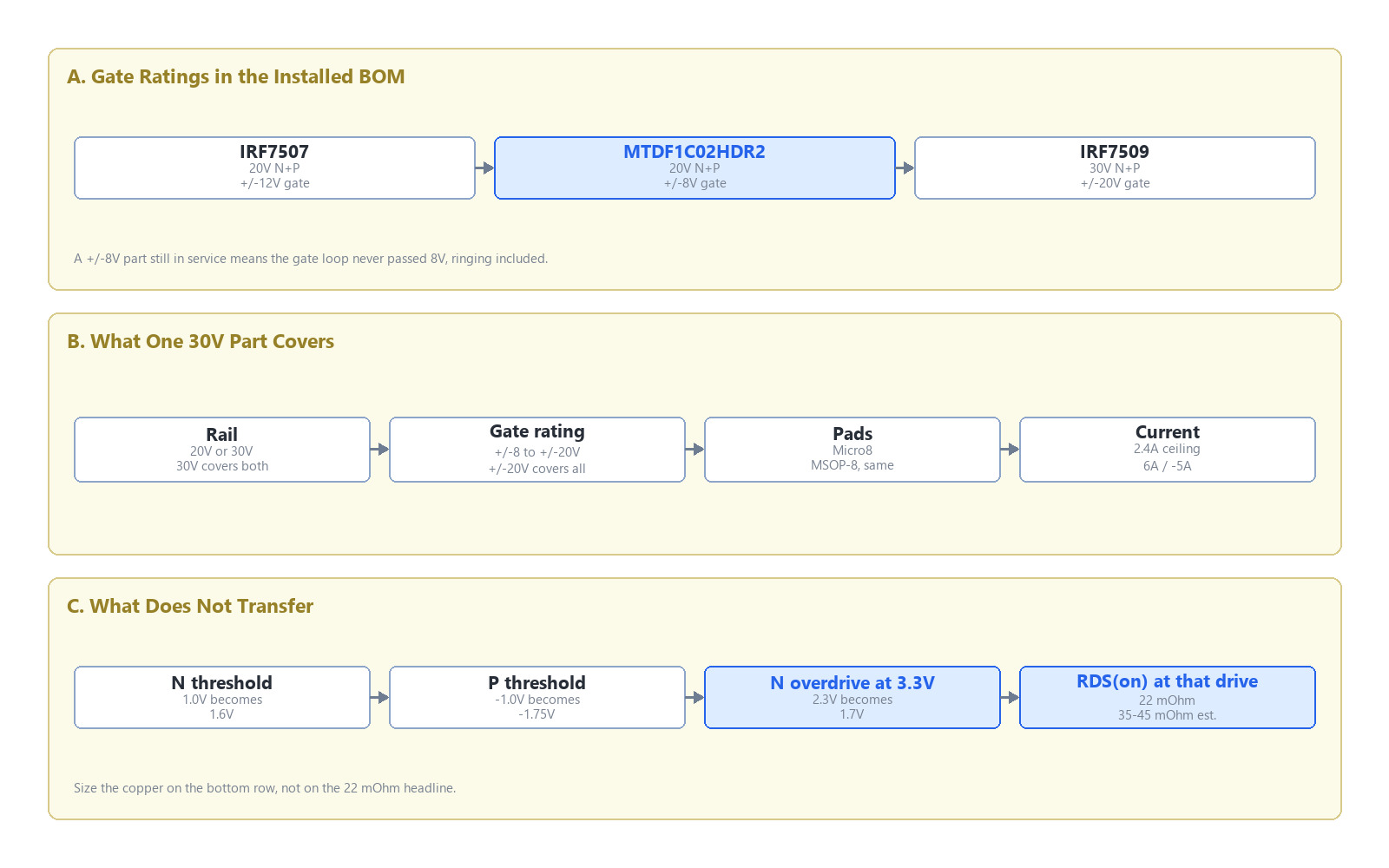
Figure 1. The three gate ratings in the installed BOM, what a ±20V part covers, and the two threshold numbers that do not transfer. The bottom row is the one that changes how the board runs.
Parameter comparison
| Part | Channels | VDSS | ID (N / P) | RDS(on) N | RDS(on) P | VGS max | Vth | Pd | Package | Status |
|---|---|---|---|---|---|---|---|---|---|---|
| IRF7507 | N+P | 20V | 2.4A / -1.7A | 140 mΩ @4.5V | 270 mΩ @4.5V | ±12V | 0.7 / -0.7V | 1.25W | Micro8 | Discontinued |
| IRF7509 | N+P | 30V | 2.7A / -2.0A | 110 mΩ @10V | 200 mΩ @10V | ±20V | 1.0 / -1.0V | 1.25W | Micro8 | Discontinued |
| MTDF1C02HDR2 | N+P | 20V | 1A class | 120 mΩ | 175 mΩ | ±8V | logic level | Micro8 | Legacy | |
| VBA10330 | N+P | 30V | 6A / -5A | 22 mΩ @10V | 45 mΩ @10V | ±20V | 1.6 / -1.75V | 3.1 / 3.2W | MSOP-8 | Active |
Two rows deserve a second look. The Pd column jumps from 1.25W to 3.1W, which at the same 150°C junction limit implies a junction-to-ambient path near 40 K/W instead of 100 K/W; the two numbers may not share a measurement basis, so use the improvement as a direction and still compute rise from your own copper area.
The status column explains why the exercise is happening at all. The two Infineon parts are gone as catalogue items, and MTDF1C02HDR2 is listed as a preferred device in a datasheet dated 2006 that ON Semiconductor no longer promotes. Whatever the electrical case, the supply case is already decided.
The N/P asymmetry does not go away
The replacement is asymmetric by a factor of 2.05×: 22 mΩ on the N channel, 45 mΩ on the P channel. That is not a defect of this part. Every one of the originals is asymmetric in the same direction, because a P-channel die of equal area conducts worse than an N-channel one — the ratio is 1.93× for IRF7507, 1.82× for IRF7509 and 1.46× for MTDF1C02HDR2.
The practical consequence is that the hotspot does not move. The high-side P channel was the hot device before the swap and it still is after it; what changes is the temperature. At 1.2A the P channel dissipates 0.39W in the 270 mΩ original and 0.065W in the 45 mΩ replacement. Against the original's 1.25W package and 100 K/W path, that is +39°C of junction rise becoming about +7°C — the copper you added to survive the original is now doing nothing.
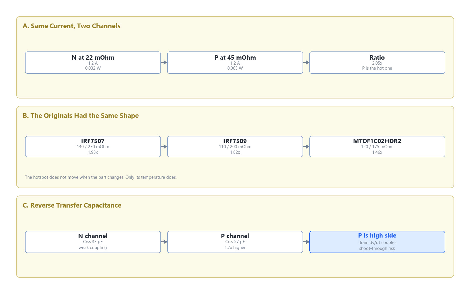
Figure 2. The P channel is the hot one in every part in this table, so the hotspot stays where it was. What changes is the junction rise, and how much of the drain's dv/dt reaches the gate through a reverse transfer capacitance that is 1.7× the N channel's.
The second asymmetry is capacitive and easier to miss. The datasheet lists 33 pF of reverse transfer on the N channel and 57 pF on the P channel. In a half bridge it is the high-side gate that sees the drain's dv/dt through exactly that capacitance, and a larger Crss means more of that edge is coupled into the gate node. If the pull-down was chosen around the coupling of the old part, it is now under-sized — and the failure mode is not a clean bang. It is a slow, temperature-dependent cross-conduction that only appears at high ambient, on the units that get shipped to the warmest market.
Same eight pads, different polarity
Every part in the table is an 8-pad surface-mount outline with the same land pattern, and that is where the danger is. On the ON Semiconductor drawing for this complementary pair, pins 1 and 2 are the P-channel source and gate, pins 3 and 4 the N-channel source and gate, and pins 5 through 8 the two drains. A dual-N part in the same outline keeps the pad geometry and puts an N channel at pins 1 and 2.
So the substitution rule is narrower than "same package". A complementary part can only be replaced by another complementary part. If a BOM carries both a dual-N device and a complementary device in MSOP-8 — which is common when one board has both a low-side pair and a half bridge — the two must not share a feeder position or a reorder code. Pick-and-place will not notice the difference. The board will, at first power-up, and the failure looks like a short rather than a wrong part.
Where this replacement stops working
Three conditions take it off the table. A rail above 30V needs a different voltage class entirely. More than 3A per channel puts the MSOP-8 outline into a thermal argument the package loses, and a SO-8 or DFN8 with a real thermal pad is the honest answer. And an N channel driven from a 3.3V logic pin at tens of kilohertz with no driver — there the 1.7V of overdrive is spent mostly in the linear region, and the switching loss dwarfs whatever the lower on-resistance returned. Add a driver, or keep a part with a lower threshold.
FAQ
Is VBA10330 a drop-in for MTDF1C02HDR2 even though the gate rating goes from ±8V to ±20V?
Electrically and mechanically, yes — same N+P arrangement, same 8-pad outline, wider rail and gate ratings. What does not transfer is the assumption behind the ±8V part: check that the gate pull-down and any series resistor still give acceptable dv/dt and false turn-on margin, because the old part may have been doing that job by failing early.
Can the N channel be driven from a 3.3V GPIO?
It will enhance, with 1.7V of overdrive, but not into 22 mΩ. Expect 35 to 45 mΩ and check the junction rise on that figure. For PWM above a few kilohertz, drive it from 5V or from a gate driver.
Both 20V originals are being replaced by a 30V part. Does the higher rating cost anything?
Not in this outline. The 30V device has a lower on-resistance, a higher current rating and a wider gate rating than either 20V original. The one thing to watch is that a 30V part invites a higher rail, and the rest of the circuit — capacitors, connectors, the motor's back-EMF clamp — was sized for 20V.
Why does the P channel run hotter than the N channel?
Because a P-channel die of equal area has higher resistance than an N-channel one; here it is 45 mΩ against 22 mΩ. In a half bridge the P channel is also the high side, so it carries the same current through more resistance. That was already true of the originals, at ratios between 1.46× and 1.93×.
The package is identical, so why worry about the pin map?
Because a dual-N part in the same 8-pad outline puts an N channel where the complementary part has a P channel. The land pattern matches, the assembly passes, and the high-side switch never turns on — or is permanently on. Match polarity, not just footprint.

Download PDF document
 Download now


