 中文
 English

30V Portable Power P-Channel MOSFET Selection: 4 Trade-offs
 Back to previous page

A dual P-channel part in the 8-pin MSOP outline that was specified at 270 mΩ can now be replaced by one at 38 mΩ, and that 7× drop in on-resistance changes almost nothing about the circuit — at 1.5A per channel the conduction loss was never what limited the design. The four numbers that actually move are gate capacitance, threshold voltage, gate-voltage rating, and package dissipation. This applies to load-switch, level-shift and battery-path circuits drawing under 2A per channel on rails no higher than -24V, where the original device was a -20V or -30V Micro8 dual. Above 3A per channel, or where the gate hangs off a 3.3V logic pin and the channel actually switches at kilohertz rates, the MSOP-8 outline runs out of thermal and drive margin and a SO-8 or DFN part is the better answer.
At a glance
- The -20V and -30V members of this family share one footprint but not one gate rating (±12V vs ±20V), so a single -30V / ±20V device retires two BOM lines at once — provided the gate network is re-checked, which is where most substitutions quietly fail.
- The newer die is 7× lower in RDS(on) and 5× higher in input capacitance. Behind a 10kΩ gate pull-up that turns a 1.8 µs edge into a 9 µs one — harmless in a load switch, fatal in a 20 kHz channel.
- The old part is thermally limited at its own nameplate. 1.7A through 270 mΩ is 0.78W against a 1.25W package with 100 K/W junction-to-ambient: +78°C of rise before the ambient air is even counted.
Why the on-resistance is the least interesting number
Take the two datasheet rows at face value: 270 mΩ maximum on the original, 38 mΩ on the replacement, both at a 10V gate. At the 1.5A a portable load switch actually carries, that is 0.61W replaced by 0.09W. Half a watt is worth having, but on a part that was already inside its package rating it does not change the topology, the copper area, or the failure mode.
What does change is the gate. A 7× reduction in RDS(on) comes from a die with roughly 7× the area, and gate charge scales with area, not with on-resistance. The original specifies 180 pF of input capacitance and 11 nC of gate charge; the replacement specifies 900 pF and 17 nC. If the gate node is driven by a real driver, this is a non-event — 17 nC at 20 mA is under a microsecond. If the gate node is pulled up through the 10kΩ resistor that was perfectly adequate for 180 pF, the edge stretches by exactly the capacitance ratio, and a circuit that switched in 2 µs now switches in 9 µs.
The second trap is the threshold. The -20V member of the family is a logic-level device with a -0.7V minimum threshold, specified down to a -2.7V gate so it enhanced fully from a 3.3V rail. The replacement's threshold is -1.7V typical. Drive it from 3.3V and there is 1.6V of overdrive, which is enough to turn on and not enough to reach the 38 mΩ the headline quotes. It will work, run hotter than the calculation says, and look like a layout problem.
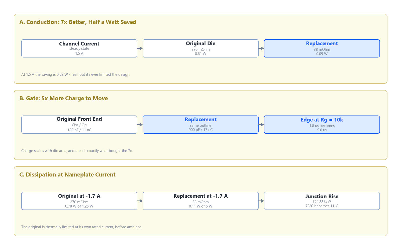
Figure 1. Conduction improves by 7×, gate capacitance grows by 5×, and the original part turns out to be thermally limited at its own rated current. The middle row is the one that costs money.
What each design variable decides
| Design variable | Old design point | Replacement | What it decides |
|---|---|---|---|
| Gate drive amplitude | 4.5V (logic-level member) or 10V | ≥4.5V, ideally 10V | Whether RDS(on) is 38 mΩ or closer to 90 mΩ |
| Gate source resistance | Often a 10kΩ pull-up | 900 pF to charge | Turn-off time; whether a PWM channel survives |
| Threshold voltage | -0.7V min / -1.0V min | -1.7V typical | Margin left on a 3.3V or 5V logic rail |
| Channel current | 1–1.5A typical | 6A rating | Conduction loss and copper area |
| Ambient | 70–85°C in a sealed enclosure | 5W package rating | Derated current, not nameplate current |
| Rail voltage | -20V or -30V | -30V, ±20V gate | Whether one SKU covers both BOM lines |
| Dissipation at rated current | 0.78W of a 1.25W budget | 0.11W of a 5W budget | Whether the part needs any copper at all |
The rail row is the one that pays for the exercise. The two original parts differ by 10V of rating and 8V of gate rating, which is why they carry two part numbers and two lines of inventory; a -30V device with a ±20V gate satisfies both, and the gate clamp that protected the ±12V part is now doing nothing but adding a resistor.
Parameter comparison
| Part | Channels | VDSS | ID | RDS(on) max | Qg typ | VGS max | Pd | Package | Status |
|---|---|---|---|---|---|---|---|---|---|
| IRF7504 | Dual P | -20V | -1.7A | 270 mΩ @ -4.5V | 5.4 nC | ±12V | 1.25W | Micro8 | Legacy |
| IRF7506 | Dual P | -30V | -1.7A | 270 mΩ @ -10V | 7.5 nC | ±20V | 1.25W | Micro8 | Obsolete |
| VBA9338 | Dual P | -30V | -6A | 38 mΩ @ -10V | 17 nC | ±20V | 5W | MSOP-8 | Active |
All three are the same 8-pin outline, so the substitution is a stencil change rather than a layout change. VBA9338 also lists 900 pF input capacitance, 185 pF reverse transfer and a -1.7V typical threshold — the three numbers that decide whether the driver on your board can still drive it.
The four trade-offs, in the order they bite
Gate charge against on-resistance. These two are the same knob turned in opposite directions. A -30V trench die at 38 mΩ is roughly seven times the silicon area of one at 270 mΩ, and every capacitance in the datasheet scales with that area: Ciss, Coss, Crss all multiply. There is no part that gives you both, so the question is not which one is better but whether your gate node has current to spare. A dedicated driver does; a microcontroller pin with a series resistor does not.
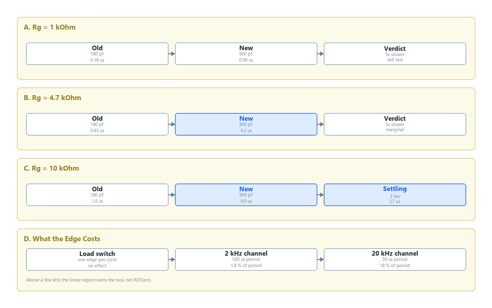
Figure 2. The same 900 pF front end is a non-event behind a 1 kΩ driver and a 9 µs edge behind a 10 kΩ pull-up. Whether that matters is set by the switching frequency, not by the device.
Threshold against logic-level operation. The original -20V part was designed for a 2.7V gate because it was aimed at battery products. If the board drives the gate from a 3.3V rail through a resistor, the replacement will conduct, but its resistance at 1.6V of overdrive is a different device from the one in the table. Either raise the drive to 4.5V, or accept a resistance two to three times the quoted figure and size the thermal path accordingly.
Voltage rating against inventory. Buying one -30V part instead of two — a -20V and a -30V — cuts a BOM line and a reorder point. The catch is that the ±20V gate rating must not be treated as permission to raise the gate drive: if the existing clamp sits at 12V, leave it there. The extra headroom is for transients on the rail, not for a redesigned driver.
Dissipation against package. The 5W rating is four times the original's 1.25W, and at these currents the part no longer needs a copper pour to survive. That is a real saving on a dense board, but it also means the thermal design that used to constrain the layout has stopped doing so — and any assumption built on it, such as "the hot corner is the FET," is now stale.
Four mistakes we see on replacement boards
- Treating "same eight pins" as "same electrical behaviour." The footprint is identical and the threshold is not. On a 3.3V rail the replacement may sit at two to three times its quoted RDS(on), which reads on the bench as a layout or solder problem rather than a device problem.
- Keeping the original gate pull-up. 900 pF behind 10kΩ is a 9 µs time constant, so roughly 27 µs to settle. Fine for a load switch that turns on once per power cycle; unacceptable for a channel switching above 2 kHz, where the device spends most of its time in the linear region.
- Comparing 38 mΩ at 10V against 270 mΩ at 4.5V. The two figures in the datasheets are measured at different gate voltages, and the ratio between them is not the ratio you will measure on the board. Compare like gate drive or the comparison is theatre.
- Reading RDS(on) as an ambient-temperature number. It is a 25°C, 10V-gate maximum. A trench die at 125°C junction typically sits 1.4–1.6× higher, so the number to design copper around is nearer 55 mΩ, not 38 mΩ.
Where this replacement stops working
Three conditions take it off the table. A rail above -30V needs a different voltage class entirely. More than 3A per channel puts the MSOP-8 outline into a thermal argument that the package loses, and a SO-8 or DFN8 with a real thermal pad is the right move. And a channel that switches at tens of kilohertz from a 3.3V logic pin — no driver, no 4.5V rail — needs either a driver added or a device with the original's 180 pF front end, because the replacement's advantage in conduction is paid for in gate charge you cannot supply.
FAQ
Is this a drop-in replacement for both the -20V and the -30V original?
Yes, on the footprint. Both originals are the 8-pin MSOP/Micro8 outline, and a -30V device with a ±20V gate covers a -20V rail and a ±12V gate as well. Check the gate drive amplitude before calling it done.
Can the gate be driven from a 3.3V microcontroller pin?
For static load switching, yes. The -1.7V threshold leaves 1.6V of overdrive, so the part enhances, but its resistance will be well above the 38 mΩ quoted at a 10V gate. For anything switching above a few kilohertz, use 4.5V or more.
Why is the gate charge five times higher when the resistance is seven times lower?
Because both scale with die area. On-resistance falls as area grows, gate charge rises with it. A 38 mΩ -30V trench die is a much larger piece of silicon than a 270 mΩ one, and the capacitance figures in the datasheet follow the area directly.
What happens if the original 10kΩ gate pull-up is left in place?
The edge becomes a 9 µs time constant, about 27 µs to settle. In a load switch that is invisible. In a 20 kHz channel the device spends most of each period in its linear region, and the switching loss overwhelms whatever the lower on-resistance saved.
Does the 5W rating mean no copper is needed?
At 1.5A the part dissipates 0.09W, so a plain footprint is enough. At the 6A rating it is not — the package number assumes a thermal path, and the datasheet curve, not the headline, decides the copper area.

Download PDF document
 Download now


