 中文
 English

Dual N-Channel Micro8 MOSFET Selection: 135 mOhm at 4.5V or 10V
 Back to previous page

Three dual N-channel parts in the 8-pad Micro8 / MSOP-8 outline make up this comparison — IRF7501, IRF7503 and IRF7530, all now out of production at Infineon — and a 30V dual with 20 mΩ at 10V drive, 25 mΩ at 4.5V and a ±20V gate (VBA6317) replaces all three on the same land pattern. The interesting part of this list is not the resistance. It is that two of the three originals are specified at 135 mΩ, and one of those 135 mΩ figures was measured at 4.5V gate drive while the other was measured at 10V. Same number, same package, same 2.4A rating, 5.5V apart. In a 4.5V-driven design the part that reads 135 mΩ is really a 222 mΩ part, and the replacement's benefit is 71% larger than the headline numbers suggest. This is written for synchronous rectifiers, load switches, battery back-to-back pairs and low-side motor switches that run under 5A per channel on rails of 24V or less. Above 5A, on a rail above 30V, or on a gate driven directly from a 2.7V logic pin, this replacement is the wrong answer.
At a glance
All three originals are gone. IRF7501 and IRF7503 are both marked obsolete or discontinued at Infineon; IRF7530 is end-of-life. There is no live competitor in this group, so the question is not whether to swap but which specification to compare against.
The two 135 mΩ ratings are not the same measurement. IRF7501 quotes 135 mΩ at 4.5V gate drive; IRF7503 quotes 135 mΩ at 10V and 222 mΩ at 4.5V. Printed side by side they look identical, and on a 4.5V-driven board they differ by 64%.
Gate ratings split inside one series: the two 20V parts, IRF7501 and IRF7530, are ±12V; the 30V part, IRF7503, is ±20V. The replacement's ±20V covers all three, but it does not license a higher drive amplitude.
Two 135 mOhm parts, 5.5V apart
Read the parameter tables of IRF7501 and IRF7503 without looking at the test conditions and the two parts appear to be the same device with a different voltage class. Both are dual N-channel in Micro8, both are rated 2.4A at 25°C ambient, both dissipate 1.25W, both have a 100 K/W junction-to-ambient path, and both list 135 mΩ.
The conditions underneath that number are not the same. IRF7501 specifies 135 mΩ at VGS = 4.5V and ID = 1.7A. IRF7503 specifies 135 mΩ at VGS = 10V and ID = 1.7A, and then adds a second row: 222 mΩ at VGS = 4.5V, with the test current halved to 0.85A. That halved test current is the tell. The manufacturer did not keep the same current for the 4.5V row because the die cannot hold it there without the resistance running away.
So the honest comparison at a given gate voltage is not 135 against 135:
| Part | RDS(on) at 10V | RDS(on) at 4.5V | Change when drive drops to 4.5V |
|---|---|---|---|
| IRF7501 | not specified | 135 mΩ | — (4.5V is its rated condition) |
| IRF7503 | 135 mΩ | 222 mΩ | +64% |
| VBA6317 | 20 mΩ | 25 mΩ | +25% |
Two things fall out of that table. First, IRF7503 and IRF7501 are not interchangeable on a 4.5V board even though both say 135 mΩ: the IRF7503 there is a 222 mΩ part, 64% worse than the IRF7501 it looks identical to on paper. Second, the replacement degrades far less when the gate supply is low — 25% against 64% — because it is a trench die that reaches most of its channel at 4.5V, whereas IRF7503 is a planar design that needs 10V to get there.
The practical instruction is short. Before quoting any of these three against a replacement, measure the gate drive amplitude on the actual board. The number on the datasheet that applies to a 4.5V driver is the 4.5V row, not the headline row, and for IRF7503 those two rows differ by 87 mΩ.
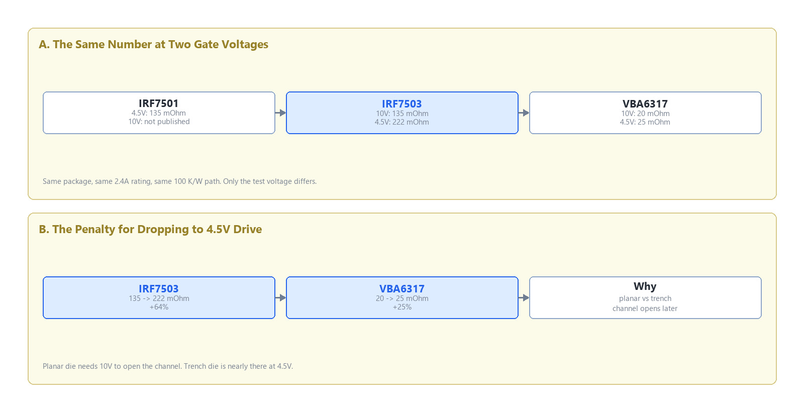
Figure 1. The same 135 mΩ figure against two different gate voltages. IRF7503 loses 64% of its conductance when the drive drops from 10V to 4.5V; the replacement loses 25%.
What a 4.5V board actually has, and what the swap really saves
Take the case that matters: a 4.5V-driven channel carrying 2A, the kind of load a synchronous rectifier or a load switch sees. On the datasheet headline, moving from IRF7503 to the replacement takes 135 mΩ down to 20 mΩ. On the board, it takes 222 mΩ down to 25 mΩ.
The difference in the saving is large enough to change the business case:
| Basis | Original RDS(on) | Replacement RDS(on) | Saving at 2A |
|---|---|---|---|
| 10V headline figures | 135 mΩ | 20 mΩ | 0.460W |
| Actual 4.5V drive | 222 mΩ | 25 mΩ | 0.788W |
The real saving is 71% larger than the one computed from the headline rows, because the part being replaced was not delivering 135 mΩ in that circuit in the first place. This is the opposite of the usual replacement risk, where the headline flatters the new part and the board disappoints. Here the headline flatters the old part and understates the gain.
There is a second-order point in the same arithmetic. At 2A and 4.5V drive, IRF7503 dissipates 0.888W against a 1.25W rating — 71% of its dissipation budget consumed by conduction alone, before switching and before any temperature derating. A part sitting at 71% of its thermal budget at 2A is not a 2.4A part in any useful sense; it is a part that has been running hot and that the designer has probably already worked around with copper or airflow without knowing why.
IRF7503 does not survive 2A at 85C in a 4.5V design
Put the thermal path on top of the resistance and the case closes hard. All three originals specify 100 K/W junction-to-ambient on the same one-inch-square board, so the same copper that keeps one of them alive keeps the others alive — and the comparison is clean.
| Part | RDS(on) at 4.5V | Loss at 2A | Rise at 100 K/W | Junction at 85C ambient |
|---|---|---|---|---|
| IRF7501 | 135 mΩ | 0.540W | 54C | 139C |
| IRF7503 | 222 mΩ | 0.888W | 89C | 174C |
| IRF7530 | 30 mΩ | 0.120W | 12C | 97C |
| VBA6317 | 25 mΩ | 0.100W | 11C | 96C |
IRF7503 lands 24°C past its 150°C limit at 2A, in an 85°C enclosure, on drive that its own datasheet calls out at 4.5V. IRF7501 gets there with 11°C to spare. The same current, the same board, the same ambient — and one of the two 135 mΩ parts fails while the other passes.
Run the question the other way and ask what current each can actually carry at 85°C ambient, which is the number a specification ought to quote but never does:
| Part | RDS(on) at 4.5V | Dissipation budget at 85C | Usable current at 85C | Rated current at 25C |
|---|---|---|---|---|
| IRF7501 | 135 mΩ | 0.65W | 2.19A | 2.4A |
| IRF7503 | 222 mΩ | 0.65W | 1.71A | 2.4A |
| IRF7530 | 30 mΩ | 0.65W | 4.65A | 5.4A |
| VBA6317 | 25 mΩ | 0.59W | 4.86A | 6.5A |
IRF7503's 2.4A rating is a 10V-drive number. In the 4.5V circuit its own datasheet describes, the part carries 1.71A before the junction reaches its limit — 29% below the nameplate. The 2.4A is not a lie; it is a statement about a gate voltage that the board may not have.
Note also that the replacement's 6.5A and IRF7530's 5.4A converge to 4.86A and 4.65A once both are referred to an 85°C ambient. A 20% gap in the ratings becomes a 4.5% gap in practice. Rated current in this package is a number about the resistance and the test board, not about what the package can take.
The thermal path is worse and it still wins
Here is the one column where the replacement loses, and it is worth naming because it is the column most engineers check first.
The replacement's steady-state junction-to-ambient is 110 K/W maximum, against 100 K/W for all three originals. On a like-for-like comparison of thermal paths the replacement is 10% worse. Anyone comparing those two numbers alone would conclude the swap makes the board hotter.
It does not, because thermal resistance and dissipation enter the junction temperature as a product, and the dissipation fell by far more than the resistance rose. At 2A the replacement dissipates 0.100W through 110 K/W for an 11°C rise; IRF7503 dissipates 0.888W through 100 K/W for an 89°C rise. An 8-fold loss reduction buries a 10% path penalty completely.
The lesson generalises to a rule worth keeping: junction-to-ambient only matters in proportion to the watts it is carrying. A part that halves its own dissipation can afford a worse path; a part that improves the path but keeps its dissipation has fixed nothing. The originals here all have identical thermal paths, which means the path never was the variable in this comparison — the resistance was.
Crss triples, Miller charge does not
The capacitance columns look alarming and mostly are not. Against IRF7503, the replacement's input capacitance is 800 pF against 210 pF, and its reverse transfer capacitance is 86 pF against 32 pF — a 2.7× increase in the capacitance that couples drain transients back into the gate.
Read the integrated figures instead and the picture changes. IRF7503 specifies 2.5 nC of gate-to-drain charge; the replacement specifies 2.7 nC. An 8% increase, against a 2.7× increase in the small-signal Crss.
Both numbers are correct, and the gap between them is the lesson. Crss is measured at a single drain voltage — 25V for IRF7503, 15V for the replacement — and it is the value near zero drain voltage that dominates the published figure, because that is where the capacitance is largest. Gate-drain charge integrates Crss across the actual switching transition, through the Miller plateau where the drain voltage is moving and the capacitance is small. A trench die with a wide channel has a lot of capacitance at low drain voltage and roughly the same capacitance in the plateau, which is exactly the pattern here: Crss up 2.7×, Qgd up 8%.
The practical consequence is that switching loss in this swap is essentially unchanged, while the small-signal coupling that governs dv/dt-induced false turn-on does get worse. Estimating switching speed from a Crss figure would have predicted a problem that does not exist; checking Qgd would have predicted correctly. When a datasheet gives both, the charge is the number that predicts the loss.
On gate drive power the arithmetic is also settled and also small. Total gate charge is 14.5 nC at 10V drive against 7.8 nC for IRF7503, an 86% increase, and at 100 kHz with a 10V amplitude that is 6.7 mW of extra drive against the 0.788W of conduction saved. It is not a consideration at any load this package can carry.
Parameter comparison
| Part | VDSS | ID at 25C | RDS(on) 10V | RDS(on) 4.5V | VGS max | Vth | Qg | Qgd | Ciss | Crss | RthJA | Pd | Status |
|---|---|---|---|---|---|---|---|---|---|---|---|---|---|
| IRF7501 | 20V | 2.4A | — | 135 mΩ | ±12V | 0.7V min | 5.3 nC at 4.5V | — | 260 pF | — | 100 K/W | 1.25W | Obsolete |
| IRF7503 | 30V | 2.4A | 135 mΩ | 222 mΩ | ±20V | 1.0V min | 7.8 nC at 10V | 2.5 nC | 210 pF | 32 pF | 100 K/W | 1.25W | Discontinued |
| IRF7530 | 20V | 5.4A | — | 30 mΩ | ±12V | 0.9V typ | 18 nC at 4.5V | 3.4 nC | — | — | 100 K/W | 1.3W | End of life |
| VBA6317 | 30V | 6.5A | 20 mΩ | 25 mΩ | ±20V | 1.6V typ | 7.1 nC at 4.5V | 2.7 nC | 800 pF | 86 pF | 110 K/W | 2.0W | Active |
Three rows in that table need to be read with their conditions attached, and each one has a footnote. IRF7501's 135 mΩ is a 4.5V figure and there is no 10V figure published, so the part cannot be credited with a conductance it was never tested for. IRF7503's 135 mΩ is a 10V figure and its 4.5V figure is 222 mΩ. IRF7530's 18 nC of gate charge is a 4.5V figure at 5.4A and is the price of its 30 mΩ — the lowest resistance on the list costs 2.5× the gate charge of IRF7503 for a third of the on-resistance.
The Vth column splits the three originals in a way that matters for direct logic drive. IRF7501 at 0.7V minimum and IRF7530 at 0.9V typical will both reach full enhancement from a 2.7V pin; IRF7530 even publishes a 45 mΩ figure at 2.7V drive, which is a statement that the part is intended for that service. The replacement's threshold is 1.6V typical, 1.2V minimum, 2.5V maximum. On a 2.7V pin that leaves 1.1V of overdrive at the typical threshold, and a device at 1.1V of overdrive is somewhere in the linear region, not at 25 mΩ.
Where this replacement stops working
Three conditions close it out.
A gate driven directly from a 2.7V logic pin with no driver. IRF7530 was specified for that service, with a 45 mΩ figure published at 2.7V; nothing in the replacement's datasheet addresses it, and at 1.6V typical threshold the overdrive is 1.1V. That is the one case in this list where the answer is to keep the original part in place or add a driver, not to recalculate.
A rail above 30V, which needs a different voltage class and a different outline. And more than 5A continuous per channel, where a 3×3 mm eight-pad package with a 100 K/W path becomes a thermal argument it loses regardless of resistance — a SO-8 or a DFN with an exposed pad is the honest answer there.
The third condition is not electrical. All four parts in this table share one land pattern, and so does the P-channel version of this same exercise. If the BOM carries both a dual N-channel and a single or dual P-channel in the eight-pad outline, they must not share a feeder or a reorder code: the assembly passes, and the failure appears at first power-up as something that looks like a short. The P-channel companion to this note, covering six single P-channel parts, is worked through in the earlier article on P-channel Micro8 replacement. The complementary branch is worse: one N die and one P die in the same eight pads, two polarities under one part number, and a mix-up shows up at power-up as a shoot-through rather than a wrong value — covered in the note on complementary N+P pairs.
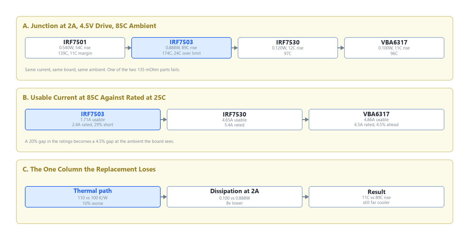
Figure 2. Dissipation and junction temperature at 2A from a 4.5V gate drive in an 85C ambient. IRF7503 crosses the 150C limit on drive its own datasheet specifies.
FAQ
Both IRF7501 and IRF7503 are listed at 135 mΩ. Why are they not equivalent?
Because the figures were measured at different gate voltages. IRF7501's 135 mΩ is specified at 4.5V drive; IRF7503's 135 mΩ is specified at 10V, and its 4.5V figure is 222 mΩ — 64% higher, with the test current for that row reduced from 1.7A to 0.85A. On a 4.5V-driven board, IRF7503 is a 222 mΩ part. Always match the test condition to the drive amplitude the board actually provides.
IRF7503 is rated 2.4A. Can it carry 2A at 85C ambient?
No, not with 4.5V drive. At 222 mΩ and 2A it dissipates 0.888W, and with the 100 K/W junction-to-ambient all three originals share, that is an 89°C rise — a 174°C junction in an 85°C enclosure, 24°C past the limit. Its practical ceiling at that ambient is 1.71A. The 2.4A rating is a 10V-drive figure.
The replacement's thermal resistance is 110 K/W against 100 K/W for the originals. Does the board get hotter?
No. Junction temperature is dissipation multiplied by resistance, and the dissipation falls 8-fold at 2A. The replacement dissipates 0.100W through 110 K/W for an 11°C rise; IRF7503 dissipates 0.888W through 100 K/W for an 89°C rise. A 10% worse path cannot compete with an 8-fold lower loss.
Reverse transfer capacitance rises from 32 pF to 86 pF. Does that hurt switching loss?
Very little. Crss is a single-point small-signal measurement taken near low drain voltage, where capacitance is largest. The integrated gate-drain charge, which is what actually flows during the Miller plateau, goes from 2.5 nC to 2.7 nC — an 8% increase. Gate charge rises 86% at 10V drive, which at 100 kHz costs 6.7 mW against 0.788W of conduction saved. Check Qgd and Qg, not Crss, when estimating switching loss.
Can one part replace a 20V and a 30V original at the same time?
For rail margin, yes — a 30V replacement adds headroom to both 20V parts. What does not transfer is the gate loop. IRF7501 and IRF7530 are both ±12V parts and IRF7503 is ±20V, inside one product series with one package, so the gate rating cannot be inferred from the resistance or the current. Keep the existing gate resistor and any clamp exactly as they are; the ±20V rating removes a limit, it does not remove the reason the limit was respected.

Download PDF document
 Download now


