 中文
 English

IRF7504 MOSFET Power Design: 20V Dual P-Channel Sizing Notes
 Back to previous page

The IRF7504 is a dual P-channel 20V part in the eight-pad Micro8 outline, rated 1.7A, 270 mΩ at 4.5V gate drive, with 8.2 nC of gate charge at maximum (5.4 nC typical), a 12V gate ceiling, and obsolete lifecycle status. A 30V dual P-channel with 38 mΩ at 10V drive, 55 mΩ at 4.5V and a ±20V gate (VBA9338) drops onto the same land pattern and cuts conduction loss five-fold at the same current. That half is arithmetic you can do in your head. The half that needs care is the gate: 8.2 nC becomes 25 nC at the same drive, three times the charge per switching event. In a load switch running below 20 kHz with a standing load under 84 mA, that tripled charge costs more than the five-fold resistance saves. Two numbers decide it, the crossover current and what 85C ambient leaves of the rating.
At a glance
The original is obsolete. IRF7504 and its ordering code IRF7504TRPBF both carry Obsolete status; there is no live 20V dual P-channel competitor to argue against.
Conduction loss at 1.2A drops from 0.39W to 0.079W, because 270 mΩ becomes 55 mΩ at 4.5V drive.
Gate charge triples, 8.2 nC maximum to 25 nC typical. Nobody looks at this number, and at low load it decides the outcome.
The swap pays off above 84 mA at 20 kHz, 188 mA at 100 kHz, 593 mA at 1 MHz. Below those currents the 270 mΩ part is the more efficient device.
The original, as specified
| Parameter | IRF7504 | Condition |
|---|---|---|
| Configuration | 2 x P-channel, Micro8 | dual, one package |
| VDS | -20V | — |
| ID at 25C ambient | -1.7A | package limited |
| RDS(on) | 270 mΩ | VGS -4.5V, ID -1.2A |
| VGS(th) | 700 mV | ID -250 uA |
| Qg | 8.2 nC max, 5.4 nC typ | VGS -4.5V |
| VGS max | ±12V | not the usual 20V |
| Ciss | 240 pF | VDS -15V |
| Pd at 25C ambient | 1.25W | implies 100 K/W |
| Status | Obsolete | base and TRPBF codes |
The 1.25W figure reads backwards as a thermal path: 150C junction minus 25C ambient is 125C, divided by 1.25W gives 100 K/W.
270 mOhm to 55 mOhm: the easy half
At 1.2A per channel the original dissipates 1.44 x 0.270 = 0.389W. The replacement at 4.5V drive dissipates 1.44 x 0.055 = 0.079W. The 0.31W difference, on a 100 K/W path, is 31C of junction temperature given away to nothing.
That is real, and for a switch carrying an amp continuously it is the whole argument. The trouble is that a 20V dual P in an eight-pad package rarely carries an amp continuously. It is more often a battery disconnect pair, a reverse-polarity block, or a load switch sitting at tens of milliamps for most of its life. There the conduction number is small enough for the gate number to overtake it.
Three times the gate charge
Gate drive loss is charge multiplied by voltage swing and frequency. At 4.5V the delta is (25 - 8.2) nC x 4.5V = 75.6 nJ per event, charged and dumped every cycle, on each channel independently. One caveat on basis: 8.2 nC is the original's maximum and 25 nC is the replacement's typical, so the two figures are not measured the same way. Same-basis typical is 5.4 nC against 25 nC, which is 4.6x rather than 3x. Using the maximum for the original makes the crossover current below smaller than it really is, so the table errs toward keeping the original.
Set that against the 0.215 Ω of conduction it saves and solve for the crossing current:
| Switching frequency | Extra gate drive power | Crossover load current |
|---|---|---|
| 20 kHz | 1.5 mW | 84 mA |
| 100 kHz | 7.6 mW | 188 mA |
| 300 kHz | 22.7 mW | 325 mA |
| 1 MHz | 75.6 mW | 593 mA |
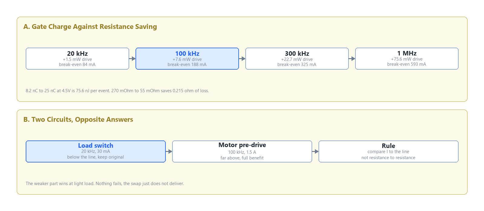
Figure 1: Where the tripled gate charge overtakes the five-fold resistance saving. Below the line the 270 mOhm original is the more efficient part; above it the swap pays.
Read it as a duty cycle question, not a datasheet question. A load switch holding 30 mA at 20 kHz sits below the 84 mA line and the replacement dissipates slightly more than the original. Nothing fails; the design just does not get the improvement it was bought for. A synchronous rectifier at 100 kHz and 1.5A sits well above it and gets the full benefit.
What 85C ambient leaves
Both parts are rated at 25C ambient. Neither will be.
| IRF7504 | VBA9338 | |
|---|---|---|
| Junction to ambient | 100 K/W | 85 K/W steady state, 50 K/W at 10s |
| Allowed dissipation at 85C | 0.65W | 0.76W |
| Usable current at 85C, 4.5V drive | 1.55A | 3.73A |
| Usable current at 85C, 10V drive | not specified at 10V | 4.49A |
The 1.7A rating survives at 85C as 1.55A, a 9% de-rating that is honest because the original's thermal path was matched to its own rating. The replacement's headline is 6A and its usable current is 3.73A, so at temperature the gap is 2.4x rather than the 3.5x the nameplates suggest.
Where this swap stops working
The driver cannot supply the charge. 25 nC needs 250 mA to switch in 100 ns. A driver picked for 8.2 nC gives a 600 ns edge where the original gave 200 ns, and a slow edge spends longer in the linear region on every transition.
The load is small and the frequency is low. Below the crossover the swap loses efficiency instead of gaining it.
The board relies on the 20V class. A 30V part adds margin, so this is not a limit. What changes is the gate loop: keep the existing gate resistor and clamp as they are. ±20V removes a limit, not the reason the limit was respected.
For the same 270 mΩ headline measured at a different gate voltage, see the dual N-channel comparison; for the P-channel Micro8 case, the 270 mOhm derating note works the usable current at 85C. The eight-pad outline all three share is on the product page.
FAQ
Can I still buy an IRF7504?
Only from channel stock. Both the base code and TRPBF are obsolete, so what circulates is inventory, and the date codes age every quarter.
Is VBA9338 a drop-in replacement mechanically?
Both are eight-pad Micro8 / MSOP-8 on the same land pattern, with the dual P-channel pinout in both. Check the pinout drawing against your layout before the first article.
Does the higher current rating mean I can raise the load?
No. 6A is at 25C case and package limited. In an 85C ambient at 4.5V drive the usable current is 3.73A.
Will the tripled gate charge show up in EMI?
It shows up as edge time first. If the driver was already marginal, a longer edge moves conducted and radiated emissions. Look at the gate waveform on the first prototype.

Download PDF document
 Download now


