 中文
 English

IRF7506 MOSFET Power Design: -30V Dual P-Channel Against a 38 mOhm Part
 Back to previous page

The IRF7506 is the case where a replacement argument cannot lean on voltage headroom. Both it and the VBA9338 are -30V dual P-channel parts in an eight-pad Micro8 outline, both take a ±20V gate. Nothing about insulation distance improves. What changes is conduction: 270 mΩ at 10V drive becomes 38 mΩ, and 450 mΩ at 4.5V becomes 55 mΩ. That is a 7.1x and an 8.2x on the same die area. The counterweight is gate charge, 7.5 nC to 50 nC at 10V, 6.7x. Solve the two against each other and the swap breaks even at 191 mA at 20 kHz, 428 mA at 100 kHz, 1.35 A at 1 MHz. Above those lines it is a straight win. Below them, the 30V original is still the better device, and it is still the device sitting in the qualification file.
At a glance
Same voltage class, so this is not a margin decision. It is a loss decision.
270 mΩ to 38 mΩ at 10V is 7.1x; 450 mΩ to 55 mΩ at 4.5V is 8.2x. The 4.5V case gains more, not less.
Gate charge at 10V goes 7.5 nC to 50 nC, so the crossover sits higher than the usual 20V swap: 191 mA rather than 84 mA at 20 kHz.
Both parts carry a ±20V gate, so the 20V-class gate loop rules do not change. That is the difference between this pair and its 20V sibling.
The original, as specified
| Parameter | IRF7506 | Condition |
|---|---|---|
| Configuration | 2 x P-channel, Micro8 | one package, two independent die |
| VDS | -30V | — |
| ID at 25C ambient | -1.7A | -1.4A at 70C |
| RDS(on) at 10V | 270 mΩ | ID -1.2A |
| RDS(on) at 4.5V | 450 mΩ | ID -0.60A |
| VGS(th) | -1.0V min | ID -250 uA |
| Qg at 10V | 7.5 nC typ, 11 nC max | ID -1.2A, VDS -24V |
| Qgd | 2.5 nC typ, 3.7 nC max | same bias |
| Ciss / Coss / Crss | 180 / 87 / 42 pF | VDS -25V, 1 MHz |
| Pd at 25C ambient | 1.25W | derating 10 mW/C |
| RthJA | 100 K/W | max |
| VGS max | ±20V | not the 12V of the 20V sibling |
Two numbers in that table are easy to misread. The 4.5V on-resistance is specified at 0.60A, not 1.2A, so it is not a like-for-like comparison with the 10V figure. And the gate charge is quoted at 10V only; the 4.5V point lives in the curve, not in the table.
30V against 30V: two numbers left
With the voltage class fixed, the loss arithmetic collapses to conduction minus gate drive.
| IRF7506 | VBA9338 | Ratio | |
|---|---|---|---|
| RDS(on), 10V drive | 270 mΩ | 38 mΩ | 7.1x lower |
| RDS(on), 4.5V drive | 450 mΩ | 55 mΩ | 8.2x lower |
| Qg, 10V drive | 7.5 nC | 50 nC | 6.7x higher |
| Qgd | 2.5 nC | 7.5 nC | 3.0x higher |
| Ciss | 180 pF | 900 pF | 5.0x higher |
| RthJA | 100 K/W | 85 K/W steady | 1.18x better |
| Current rating | 1.7A | 6A | 3.5x higher |
At 1.2A per channel, conduction falls from 0.389W to 0.055W at 10V drive and from 0.648W to 0.079W at 4.5V drive. The 4.5V case saves more watts precisely because the original is worse there.
The crossover sits higher than people expect
Gate drive delta at 10V is (50 - 7.5) nC x 10V = 425 nJ per switching event, per channel. Set that against the 0.232 Ω of conduction removed and solve:
| Switching frequency | Extra gate drive power | Crossover load current |
|---|---|---|
| 20 kHz | 8.5 mW | 191 mA |
| 100 kHz | 42.5 mW | 428 mA |
| 300 kHz | 127.5 mW | 741 mA |
| 1 MHz | 425 mW | 1.35 A |
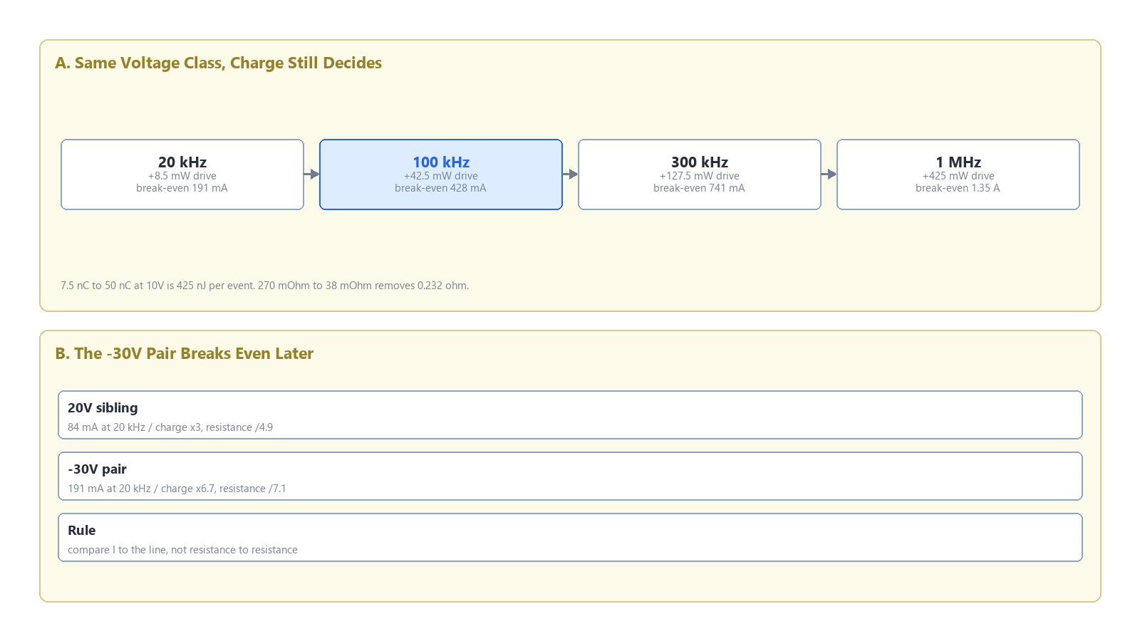
Figure 1: The crossover line for a same-voltage swap. Resistance improves 7.1x but gate charge rises 6.7x, so the break-even current is 2.3 times higher than the 20V case at the same frequency.
Compare with the 20V sibling: 84 mA at 20 kHz. The -30V pair breaks even at 191 mA, 2.3 times higher, because the charge penalty grew faster than the resistance gain. A designer who sized the 20V swap at 30 mA of load and concluded "keep the original" will get the opposite answer here at 300 mA.
The 4.5V point the table does not give
IRF7506 switches at 4.5V with a threshold of -1.0V minimum, so 4.5V is only 3.5V of overdrive, and the 450 mΩ figure is the honest one at that bias. The replacement at 55 mΩ is 8.2x better there.
What the datasheet does not give is the 4.5V gate charge. The table quotes 7.5 nC at 10V, and the 4.5V point has to be read off the gate charge curve, or estimated from the plateau. Estimating it as roughly 3.5 nC changes the delta from 42.5 nC to 21.5 nC and drops the 20 kHz crossover from 191 mA to about 136 mA. Any design that runs 4.5V drive and sits between those two currents should measure rather than assume.
Qgd and Crss do not move together
Crss rises 4.4x, from 42 pF to 185 pF, while Qgd only rises 3.0x, from 2.5 nC to 7.5 nC. The reason is that Qgd is the charge moved across the Miller plateau, and the plateau width scales with the drain voltage swing over the current, not with capacitance alone. A part with more Crss but proportionally more transconductance moves the same charge across a shorter plateau.
The practical consequence points two ways. Higher Crss means more Miller feedback, which limits dv/dt and quiets the switching node; higher Qgd means more energy in every transition. The two effects pull in opposite directions on EMI and the same direction on switching loss, so the oscilloscope matters more than the datasheet here.
For the 20V version of this same swap, where the gate ceiling does change, the sibling's derating note works the usable current. For the test conditions behind a headline on-resistance, the dual N-channel comparison covers it.
Where this swap stops working
Load under 190 mA at 20 kHz. Below the crossover the extra charge costs more than the resistance saves, and it costs it continuously.
A driver sized for 7.5 nC. 50 nC in 100 ns needs 500 mA of gate current. A driver picked for the original gives a 670 ns edge, and a slow edge spends longer in the linear region on every transition.
A layout that leans on the original's Crss. The extra Miller capacitance changes ringing and snubber values. Re-check the drain node on the first prototype rather than carrying the old RC values over.
FAQ
Is this a drop-in replacement?
Electrically and mechanically yes: same Micro8 land pattern, dual P-channel pinout, ±20V gate on both, -30V on both. The part that changes is the gate drive budget.
Why is the 4.5V gain larger than the 10V gain?
Because the original degrades faster at low gate voltage. 450 mΩ against 55 mΩ is 8.2x, while 270 mΩ against 38 mΩ is 7.1x.
Can I drive it from a 3.3V rail?
No. At 3.3V the overdrive over a -1.0V threshold is too small for either part to reach its specified on-resistance. Use a driver that pulls the gate to at least 4.5V.
Does the 6A rating triple the usable current?
At 85C ambient with 85 K/W, the replacement carries 3.73A at 4.5V drive against 1.55A for the original, so 2.4x rather than 3.5x.

Download PDF document
 Download now


