 中文
 English

IRF7726TRPBF P-Channel MOSFET Replacement: Can VBA8338 Drop In
 Back to previous page

IRF7726TRPBF is a single P-channel in Infineon's Micro8 package: 3 x 3 mm, 0.91 mm tall, -30V, 26 mOhm, a 7A part. It appears in the same places as the 90 mOhm IRF7606TRPBF from the same family, only one current class up: the battery master switch in a handheld or a power tool, the power path between the pack and the system, the high-current load switch behind a USB port or a motor branch, and the transfer between a battery and an adapter. What these share is that the position conducts all the time and the gate rarely moves, but the current runs from 3A to 6A, and the board still leaves only 1.2 mm of clearance for a power device.
Infineon issued a FIT report in 2022, a product qualification report in 2023, and the part is still listed in the 2026 small-signal selection guide, so it has not been discontinued. What follows covers one question: under what conditions VBA8338 can replace it.
The part that can replace it is VBA8338: also -30V, also a +/-20V gate, also a 3 x 3 mm eight-lead package, with 18 mOhm at 10V drive and a gate charge of only 25nC. Resistance and charge both improve, but the current rating on the front page is a notch lower and the steady-state thermal resistance is higher. The differences fall in three places: which of the four positions takes the swap directly, which needs the current recomputed, and why the substitute datasheet carries two thermal numbers.
What changes
Resistance improves at both drive voltages. At 10V it falls from 26 mOhm to 18 mOhm, down 31%; at 4.5V from 40 mOhm to 25 mOhm, down 37%. The low-voltage gain is larger, and 4.5V is exactly where a 3.3V system operates.
Gate charge falls from 46nC to 25nC, down 46%, and input capacitance from 2204pF to 1600pF, down 27%. This one favours the swap, opposite to the previous generation.
The current rating is a notch lower: -7.0A against -6.0A at 25C ambient, -5.7A against -4.6A at 70C ambient. Any position carrying more than 4A has to be recomputed.
The thermal resistance has two readings, and only the substitute carries both. The original gives one number across the whole datasheet: 70 C/W, and its power-derating table is derived from it. The substitute's thermal table reads 40 C/W typical and 50 C/W maximum for 10 seconds or less, a footnote on the same page gives a steady-state limit of 95 C/W, and its power-derating table is derived from 50 instead. A position that conducts all the time takes the steady-state number, so this article works with 95 against 70.
On the steady-state number, at 3A the original rises 16C and the substitute 15C. Almost flat. Temperature rise stays flat and the loss is what falls: 0.234W against 0.162W at 3A.
Circuit positions
The position comes first, because the same part number in different positions gives different answers. This device shows up in four places, almost exclusively.
| Position | How it is connected | What the device must do |
|---|---|---|
| Battery master switch / power path | Source toward the system, drain toward the pack, gate pulled to ground through a resistor | Conducts continuously, so conduction loss turns straight into heat; leakage must be low when off |
| High-current load switch (USB port, motor branch, peripherals) | Source toward the load, gate pulled low by an MCU or a dedicated driver | Survive the inrush at turn-on; keep the static drop off the load |
| Battery-to-adapter OR-ing | Two devices back-to-back or common-drain, gates cross-controlled | Thresholds must match; neither body diode may conduct in reverse |
| Isolation of a 4.5V or lower rail | In series with the rail, gate tied to a logic level | Still low resistance at 4.5V or even 2.5V gate drive |
All four share one property: the device conducts continuously and does not switch. Switching loss is irrelevant in a circuit that switches a few times a year, and what decides whether the part works is conduction drop and heat. Every calculation below is about those two.
Channel type and package
Channel type: There is no charge pump at a high-side position. An N-channel on the high side needs its gate a dozen volts above the source to be fully on, which means a bootstrap capacitor or an isolated driver. A P-channel opens by pulling its gate to ground. In a portable device, deleting that driver path deletes a chip, a handful of capacitors and a layout problem. The price is that a P-channel is inherently two to three times more resistive than an N-channel of the same area, which is why the P-channels in this position are pushed to the 3 x 3 mm limit rather than something smaller.
Single P against dual P: A dual package carries two dice that can each take a path: one for reverse-polarity blocking, one for system disconnect, or one per source in an OR-ing pair. Area and cost both double. IRF7726 is single P, so it fits the case of one high-current path that is switched as one. If the circuit needs two independently controlled devices, this part needs a companion.
Package height: Micro8 and MSOP8 are both 3 x 3 mm and under 1.1 mm tall; SO-8 is 5 x 4 mm and 1.75 mm. Phones, earbud cases and handheld instruments routinely leave 1.2 mm of clearance for power devices, and an SO-8 hits the enclosure. A replacement in this position has to match the package exactly; an SO-8 is not a workable compromise.
Against the 90 mOhm class: Both are Micro8 single P-channels, but IRF7606TRPBF is the 90 mOhm, 3.6A class and IRF7726TRPBF is the 26 mOhm, 7A class, the high-current end of this family. It belongs to the battery-path class and is not used for low-current positions. Size it for the 7A case, not for 3.6A.
Parameter comparison
The full comparison, datasheet figures only:
| Parameter | IRF7726TRPBF | VBA8338 | Change |
|---|---|---|---|
| Package | Micro8 (3x3 mm) | MSOP8 (3x3 mm) | Footprint compatible |
| VDSS | -30V | -30V | Same |
| VGS rating | +/-20V | +/-20V | Same |
| RDS(on) at -10V | 26 mOhm | 18 mOhm | 31% lower |
| RDS(on) at -4.5V | 40 mOhm | 25 mOhm | 37% lower |
| ID at TA=25C | -7.0A | -6.0A | One notch lower |
| ID at TA=70C | -5.7A | -4.6A | One notch lower |
| VGS(th) | -1.0V min / -2.5V max | -1.7V max | Ranges nearly coincide |
| Qg at -10V | 46nC (max 69nC) | 25nC (max 38nC) | 46% lower |
| Ciss | 2204pF | 1600pF | 27% lower |
| RthJA (10 s or less) | 70 C/W | 40 C/W typical, 50 C/W max | Better |
| RthJA (steady state) | 70 C/W | 95 C/W (footnote c) | 36% worse |
| Pd at TA=25C | 1.79W | 2.5W | Figure improves |
| Status | Active | Active |
The 4.5V drive gains more: Gate drive in 3.3V systems usually sits near 4.5V, and there the original is 40 mOhm against 25 mOhm for the substitute. At 3A the drop falls from 0.12V to 0.075V and the loss from 0.36W to 0.225W. Move to a 10V drive and the same swap is worth 31% instead of 37%. The resistance drop is 37% in a 4.5V system and 31% in a 10V one.
Gate charge is lower: 46nC against 25nC, and drive loss scales with Qg times drive amplitude times frequency: at 10V drive and 100kHz, drive loss falls from 46uW to 25uW. The substitute is also faster on the switching side, but switching times cannot be compared directly. Infineon measures at Rg=6Ω, VBsemi measures at Rg=1Ω; a gate resistor six times smaller switches off faster for obvious reasons. The comparable figure is the charge.
Steady-state thermal resistance is higher: On the short-duration number it is 70 against 50, so the substitute is better; the footnote on the same page gives a steady-state limit of 95 C/W. A battery path conducts all the time, so steady state is the condition it actually lives in, and on that number the substitute is worse.
Both thermal figures applied side by side, with a 150C junction limit:
| Current | Loss, original | Loss, substitute | Rise, original (70 C/W) | Rise, substitute (95 C/W) |
|---|---|---|---|---|
| 3A | 0.234W | 0.162W | 16C | 15C |
| 4A | 0.416W | 0.288W | 29C | 27C |
| 5A | 0.650W | 0.450W | 46C | 43C |
| 6A | 0.936W | 0.648W | 65C | 62C |
Resistance falls 31% and steady-state thermal resistance rises 36%; the two cancel, so temperature rise stays flat and the loss is what falls. At 3A the 0.072W difference is about 0.6 percentage points of system efficiency on a 3.7V pack feeding 3A.
Folded to an 85C ambient, usable power is (150 minus 85) divided by thermal resistance: 0.93W on the original, which is 5.98A, and 0.68W on the substitute, which is 6.16A but is capped by the -6.0A board rating in the datasheet. At 85C both parts land at about 6A, so the substitute holds no current advantage. The lower rating needs separate treatment.
The four positions
Battery master switch / power path, swap directly below 4A: The position conducts continuously, so the lower Qg and Ciss cost nothing. The lower resistance turns straight into efficiency. What has to be checked is the load current: if the path carries 5A continuously, the rise approaches 46C and the substitute's thermal disadvantage starts to show, so run both parts' steady-state thermal resistances for that position. The gate pull-down resistor does not need to change; the two threshold ranges nearly coincide.
High-current load switch (USB port, motor branch, peripherals), swap but recompute the inrush: Lower on-resistance means a higher peak when a capacitive load is plugged in, since peak current is bus voltage divided by on-resistance plus loop resistance plus capacitor ESR. If the original's 26 mOhm was doing incidental current limiting, the substitute removes that. Either add soft-start or put a small resistor at the source.
Battery-to-adapter OR-ing / reverse-polarity blocking, check the threshold and the body-diode direction: Back-to-back and common-drain structures rely on thresholds and body-diode direction working together. The two threshold ranges nearly coincide, so the handover point does not move much, which is good news. The body diode needs attention: the original is rated for -1.8A of continuous source current and the substitute for -2.1A, neither of them large, and both forward drops are capped at -1.2V. If this position blocks in reverse, the body diode on the conducting side has to hold the reverse voltage; do not look at the gate alone.
Isolation of a 4.5V or lower rail, the largest gain of the four: The original is 40 mOhm at 4.5V drive and the substitute 25 mOhm, 37% lower. Watch the lower limit of the drive voltage: the two threshold maxima are -2.5V and -1.7V, so with the gate tied to a 2.5V logic pin the overdrive is only 0.5V to 0.8V, both parts sit in the linear region and the real resistance is far above the specified value. Either add a driver stage or leave both parts alone.
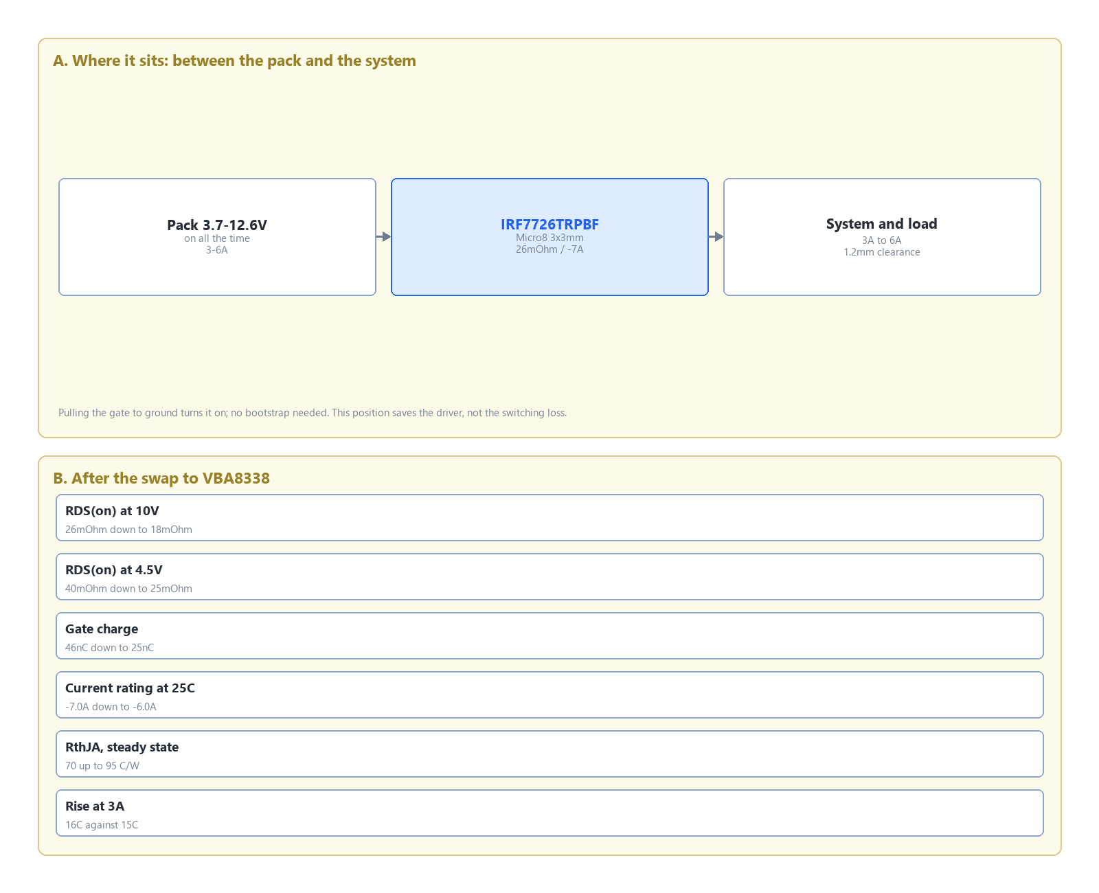
Figure 1. IRF7726TRPBF sits on the path between the pack and the system. After the swap to VBA8338 the resistance at 10V drive falls 31% and the gate charge falls 46%, but the current rating drops a notch and the steady-state junction-to-ambient thermal resistance rises from 70 C/W to 95 C/W, so the temperature rise at 3A stays about the same.
Checks before the swap
What the continuous current on this path is. Below 4A the difference is pure efficiency and the swap is free. Between 4A and 6A, work out the rise for each part from its own steady-state thermal resistance before deciding. Above 6A the package itself is at its ceiling and no substitution rescues it.
What the gate drive voltage is. At 4.5V and above the substitute's 25 mOhm is sound, and that is where the gain is largest. At 2.5V to 3.0V direct drive both parts are in the linear region; do not swap.
Whether this device is a path or a switch. As a path, judge it on conduction loss and temperature rise. As a switch, judge it on gate charge, and there the substitute wins clearly: 46nC against 25nC.
How much copper the board gives. Both datasheets assume a 1-inch-square test board. Less copper means a higher thermal resistance and the 85C line has to move down, and with only eight leads this package suffers from thin copper more than a large one does.
Whether the BOM also carries an N-channel in the same package. A 3 x 3 mm eight-lead P-channel and N-channel share a footprint. The pick-and-place will not complain; the first power-up will.
When the swap does not apply
Continuous current above 6A: That is the thermal ceiling of a 3 x 3 mm eight-lead package, and 18 mOhm does not change the package. More current means a thermal-pad SO-8 or DFN, not another part in this footprint.
A rail above 30V: Both are -30V parts; at 80% derating that is a 24V rail. Beyond that you need a different voltage class, and the package changes with it.
The gate tied to a 2.5V or 2.7V logic pin with no driver stage: This is the one case where every electrical parameter appears to pass and the swap still fails in the field: both parts sit in the linear region, and the substitute is simply the more expensive one.
Swapping only to save a little on procurement, with nothing else checked: The original can be bought and delivered, and the 31% resistance improvement has to land as efficiency to pay for itself. If the path is re-sourced once every few years, spending that on 0.07W of loss plus a re-qualification plus the risk of a wrong part is not worth it.
Going straight from the 90 mOhm class to this 7A class in one step: That is not a substitution, it is a redesign: gate drive, inrush, board copper and protection all have to be reviewed again.
FAQ
Is IRF7726TRPBF discontinued, and can it still be bought? No, it is in production. Infineon's recent FIT report, product qualification report and small-signal selection guide all still list it. The value of the substitute is its 18 mOhm resistance, its 25nC gate charge and a stable supply, not rescue from an allocation.
The current rating goes from 7A to 6A, so why does the swap still work? Both ratings are board-level figures on a 1-inch-square board under the same conditions, and the missing 1A is not what the loss difference explains. Folded to an 85C ambient, the two parts both land at about 6A. What does separate them is efficiency: 0.162W against 0.234W at 3A, and 31% lower resistance at 10V drive.
Why does the gain differ between 4.5V and 10V drive? IRF7726TRPBF is 40 mOhm at 4.5V drive and 26 mOhm at 10V; VBA8338 is 25 mOhm and 18 mOhm respectively. The ratios are 1.6 and 1.44. The low-voltage class is the one that suffers, so the substitute has more relative ground to win there.
The two datasheets use different thermal conventions. Which one do I design with? Infineon's IRF7726TRPBF gives a single junction-to-ambient figure, 70 C/W, and its power-derating table is derived from it. The VBA8338 thermal table reads 40 C/W typical and 50 C/W maximum for 10 seconds or less, a footnote gives a steady-state limit of 95 C/W, and the power-derating table is derived from 50 instead, so the two numbers in that datasheet contradict each other. A battery path conducts continuously, so take the conservative steady-state value: 70 C/W against 95 C/W.
Is the switch really ten times faster, from 227 ns down to 23 ns? No, those two cannot be compared. Infineon measures switching time at Rg=6Ω and RD=15Ω, VBsemi measures at Rg=1Ω, a gate resistor six times apart. The comparable figure is the gate charge: 46nC typical for IRF7726TRPBF against 25nC typical for VBA8338.
Does the circuit need changes after the swap? Two of the four positions need none. The high-current load switch needs soft-start or a source resistor, and the 4.5V-and-below rail needs its drive margin checked. The battery master switch needs nothing as long as the load stays below 4A.

Download PDF document
 Download now


