 中文
 English

VBA2305 MOSFET Replacement for FDS6681Z and Si4459ADY: Ratings
 Back to previous page
FDS6681Z and Si4459ADY are both 30V P-channel MOSFETs in an SO-8. At a 10V gate drive the first is 3.8 mOhm typical and 4.6 mOhm maximum with a -20A continuous rating at 25C ambient; the second is 3.9 mOhm typical and 5.0 mOhm maximum with -29A at a 25C case. Their datasheets list the same applications: adapter and charger switches, battery switches, load switches, notebook power-path control.
Bills of materials treat the two as one grade and buy whichever is in stock. Replacement work breaks that assumption quickly: 5V of gate rating, 9A of current rating, 30 C/W of steady-state thermal resistance and 56 nC of gate charge separate them.
The candidate is the VBA2305, same package and same voltage class: 30V, 5.0 mOhm typical at 10V, 8.0 mOhm typical at 4.5V, -18A at a 25C case, -11A for 10 seconds on a one-square-inch board.
Three items need checking one at a time: a typical-only on-resistance, a gate charge quoted from the 4.5V column, and current ratings carrying two different time bases. None of them affects soldering. All of them affect whether the part still holds the margin the design was built on.
Where It Sits
| Position | How it is connected | Current range | What matters |
|---|---|---|---|
| Discharge switch in a 1S or 2S pack | In series between pack and system, source to pack positive, gate pulled low by a protector or charge pump | 3A to 15A | Gate rating, steady-state thermal resistance |
| Adapter and charger input switch | Two devices back to back in the input rail, gate driven by adapter detection | 2A to 8A | Body diode direction, gate charge |
| Load switch | Single high-side device, gate driven by the charge pump inside a load-switch IC | 1A to 10A | Soft-start time, gate charge |
| Notebook power-path switching | Transfer device between battery and adapter | 5A to 20A | Conduction loss, package cooling |
All four conduct for long periods and switch rarely. Conduction is about resistance and thermal resistance; switching is about gate charge and gate rating. The three differences below split along that line.
The Two Originals Are Not Equivalents
| Item | FDS6681Z | Si4459ADY |
|---|---|---|
| Gate rating | ±25V | ±20V |
| On-resistance at 10V (typ / max) | 3.8 / 4.6 mOhm at -20A | 3.9 / 5.0 mOhm at -15A |
| On-resistance at 4.5V (typ / max) | 5.2 / 6.5 mOhm at -17A | 6.2 / 7.75 mOhm at -10A |
| Continuous current at 25C case | not listed separately | -29A |
| Continuous current at 25C ambient | -20A, 1 in2 2 oz copper, steady state | -19.7A, 1 in2 board, 10 seconds |
| Junction-to-ambient, steady state | 50 C/W | 80 C/W |
| Gate charge at 10V | 185 nC typ / 260 max | 129 / 195 nC |
| Gate charge at 4.5V | 105 / 150 nC (listed at 5V) | 61 / 95 nC |
| Input capacitance | 7540 pF | 6000 pF |
| Threshold (min / typ / max) | -1.0 / -1.8 / -3.0V | -1.0 / not given / -2.5V |
| Single-pulse avalanche energy | not rated | 45 mJ at -30A |
The ±25V figure is a feature line in the FDS6681Z datasheet, written for battery applications that let the gate swing wider. Si4459ADY stops at ±20V. Both are called 30V SO-8 parts in the 5 mOhm class, but one tolerates 25V on the gate and the other does not. This is the easiest difference to miss, because the two numbers never appear in the same row of any comparison table.
The current row is messier. FDS6681Z publishes a single -20A figure, anchored to a one-square-inch 2 oz copper pad at steady state. Si4459ADY publishes -29A at a 25C case and -19.7A at 25C ambient for 10 seconds. Same package, one figure is a steady-state ambient rating and the other is a case rating; the 9A gap is not a 9A gap in silicon.
Avalanche: Si4459ADY carries 45 mJ, FDS6681Z has no such row. Unrated does not mean incapable, but there is no number to design against, so a position that switches an inductive load has to be held to the Si4459ADY line.
The Replacement Publishes Typical Only
| Item | FDS6681Z | Si4459ADY | VBA2305 |
|---|---|---|---|
| Test current at 10V | -20A | -15A | -15A |
| Typical at 10V | 3.8 mOhm | 3.9 mOhm | 5.0 mOhm |
| Maximum at 10V | 4.6 mOhm | 5.0 mOhm | not published |
| Typical at 4.5V | 5.2 mOhm | 6.2 mOhm | 8.0 mOhm |
| Maximum at 4.5V | 6.5 mOhm | 7.75 mOhm | not published |
| At 125C junction | 5.0 / 6.3 mOhm | not given | not given |
Column against column: typical against typical, the replacement's 5.0 mOhm is 32% above 3.8 mOhm and 28% above 3.9 mOhm. Maximum against maximum, there is nothing to compare, because the only number printed sits in the typical column, and it happens to equal Si4459ADY's maximum.
The summary page is where this gets misread. It puts FDS6681Z's 4.6 mOhm next to the VBA2305's 5.0 mOhm, a 0.4 mOhm difference. One of those is a guaranteed ceiling and the other is a typical. Compared in the same column, the replacement's typical value has already crossed the original's maximum.
Volume design has to work from the worst case. With no maximum published, the next best step is to take the typical and add 20%: 6.0 mOhm as a design value. That is 30% above FDS6681Z's 4.6 mOhm and 20% above Si4459ADY's 5.0 mOhm.
The test-current column does not favour the replacement either. FDS6681Z's 3.8 mOhm was measured at -20A, the other two at -15A, and P-channel resistance rises with current, so normalising to one current widens the gap rather than closing it.
Gate Charge: The Summary Uses the 4.5V Column
| Item | FDS6681Z | Si4459ADY | VBA2305 |
|---|---|---|---|
| At 10V drive (typ / max) | 185 / 260 nC | 129 / 195 nC | 56 / 84 nC |
| At 4.5V drive (typ / max) | 105 / 150 nC | 61 / 95 nC | 27 / 41 nC |
| Number on the summary page | 185 nC | 61 nC | 27 nC |
Both Si4459ADY and VBA2305 print the 4.5V typical on the summary page; FDS6681Z prints the 10V figure. So "27 against 61 against 185" compares three numbers taken at two different gate drives.
Normalised to 10V: 56 nC against 129 and 185. The replacement is 57% below Si4459ADY and 70% below FDS6681Z.
Normalised to 4.5V: 27 nC against 61 and 105, which is 56% and 74% lower.
The benefit lands where the gate driver is weak. Load-switch ICs commonly deliver tens of microamps from a charge pump. At 50 uA, charging 185 nC to 4.5V takes 3.7 ms, 129 nC takes 2.6 ms, 27 nC takes 0.54 ms. Soft-start time and the linear-region loss during turn-on follow that number. On a board with a dedicated gate driver delivering amp-level peaks, the advantage is worth nothing.
Threshold and 3V Drive
| Item | FDS6681Z | Si4459ADY | VBA2305 |
|---|---|---|---|
| Threshold minimum | -1.0V | -1.0V | -1.0V |
| Threshold typical | -1.8V | not given | not given |
| Threshold maximum | -3.0V | -2.5V | -2.2V |
| On-resistance at 2.5V | not given | not given | not given |
When the gate of a high-side P-channel device is pulled to ground, the gate-source voltage equals the pack voltage. A 1S lithium pack at 3.0V therefore drives the gate with 3.0V, and what remains after subtracting the threshold ceiling is the overdrive: zero for FDS6681Z, 0.5V for Si4459ADY, 0.8V for the replacement.
Zero overdrive at the worst case means the device is not guaranteed to turn on. That is a common failure at the end of a 1S discharge, and it shows up as output droop and local heating. This is one of the few columns where the replacement leads.
The cost is that no on-resistance is published in that region on any of the three datasheets, so 0.8V of overdrive cannot be converted into a resistance figure without bench measurement. Positions running 2S or higher, or driving the gate to -6V from a charge pump, never see this item.
Four Current Ratings
| Item | FDS6681Z | Si4459ADY | VBA2305 |
|---|---|---|---|
| 25C case | not listed | -29A | -18A |
| 70C case | not listed | -23.5A | -13A |
| 25C ambient | -20A (steady state) | -19.7A (10 s) | -11A (10 s) |
| 70C ambient | not listed | -15.6A (10 s) | -8A (10 s) |
| Pulsed, 100 us | -105A | -70A | -145A |
| Power dissipation at 25C case | 2.5W | 7.8W | 5.6W |
At the same 25C ambient, one part is rated -20A indefinitely and another -11A for ten seconds. Placing those two numbers side by side in a selection table compares a steady-state figure against a transient one, and the conclusion tilts one way.
The replacement's four lines are -18A at a 25C case, -13A at a 70C case, -11A at 25C ambient for 10 seconds, and -8A at 70C ambient for 10 seconds. The case lines assume heat leaves through the case; the ambient lines assume it leaves through the board and only for ten seconds. On a board with no heatsink, only the last two apply.
Rise at the Same Current
| Item | FDS6681Z | Si4459ADY | VBA2305 |
|---|---|---|---|
| Junction-to-ambient, 10 s | not listed | 35 C/W max | 40 C/W max |
| Junction-to-ambient, steady state | 50 C/W | 80 C/W | 85 C/W |
| Junction-to-foot, steady state | 25 C/W | 16 C/W max | 22 C/W max |
Estimating with dT = I squared times on-resistance times thermal resistance, using 25C resistance values (maximum for the originals, typical for the replacement), all on one basis:
| Current | FDS6681Z | Si4459ADY | VBA2305 |
|---|---|---|---|
| 10A | 23.0C | 40.0C | 42.5C |
| 15A | 51.8C | 90.0C | 95.6C |
Coming from a Si4459ADY position, the junction runs 2.5C hotter at 10A. Coming from an FDS6681Z position, it runs 19.5C hotter. The dominant term is not resistance, it is thermal resistance: 85 against 50 is 70%, while resistance differs by 32%.
FDS6681Z publishes one junction-to-ambient figure of 50 C/W with no split between the ten-second and steady-state cases, so that cell is left blank. The same 50 C/W is specified for 2 oz copper, while the other two say one square inch of FR4 board without stating copper weight. One step of copper weight moves thermal resistance by 20 to 30%, so 50 should not be used as an absolute. But 50 against 85 is a 70% gap, which copper weight does not explain, so the direction holds.
The estimate above uses 25C resistance, and hot resistance is higher, so only the relative differences should be read from it. To size current properly, work backwards from 85 C/W, a 150C junction limit and a 60C ambient: 1.06W allowed, which at 5.0 mOhm is 14.5A; at 7.0 mOhm after a 1.4x temperature factor, 12.3A. That lands close to the datasheet's -11A for ten seconds, which suggests -11A is not a conservative number but the real order of magnitude for this package on this board.
Three Ways to Proceed
The first: the position holds a Si4459ADY, actual current stays under 10A, the drive is 10V or 4.5V, and the gate never exceeds 20V. Replace directly. Thermal resistance differs by 5 C/W, resistance is 28% higher on the same basis, gate charge is half. This is the easy case.
The second: the position holds an FDS6681Z. It can be replaced, with two additions. Clamp the gate to 20V, because the 25V allowance is gone. And recompute cooling at 85 C/W: 19.5C hotter at 10A, 43.8C hotter at 15A. What comes back is 70% less gate charge and 54% less input capacitance.
The third: continuous current above 15A. Do not replace. This part's steady-state capability sits between 11A and 12A, and 15A at 85 C/W already means 95C of rise, which a 60C ambient cannot absorb. The same voltage class offers the VBQA2302, a DFN8 5x6 part rated -120A at 2.2 mOhm, at the cost of a new land pattern.
Full Parameter Comparison
| Parameter | FDS6681Z | Si4459ADY | VBA2305 |
|---|---|---|---|
| Package | SOIC-8 | SO-8 | SOP8 |
| Channel | P | P | P |
| Voltage rating | -30V | -30V | -30V |
| Gate rating | ±25V | ±20V | ±20V |
| Threshold (min / typ / max) | -1.0 / -1.8 / -3.0V | -1.0 / - / -2.5V | -1.0 / - / -2.2V |
| 10V on-resistance (typ / max) | 3.8 / 4.6 mOhm | 3.9 / 5.0 mOhm | 5.0 / not published |
| 4.5V on-resistance (typ / max) | 5.2 / 6.5 mOhm | 6.2 / 7.75 mOhm | 8.0 / not published |
| Continuous current at 25C case | not listed | -29A | -18A |
| Continuous current at 25C ambient | -20A | -19.7A | -11A |
| Pulsed current | -105A | -70A | -145A |
| Body diode current at 25C case | -2.1A | -6.5A | -5A |
| Body diode drop (typ / max) | -0.7 / -1.2V | -0.71 / -1.2V | -0.73 / -1.1V |
| Gate charge at 10V / 4.5V | 185 / 105 nC | 129 / 61 nC | 56 / 27 nC |
| Input capacitance | 7540 pF | 6000 pF | 3490 pF |
| Output capacitance | 1400 pF | 860 pF | 1420 pF |
| Gate resistance | - | 0.6 / 3 / 6 Ohm | 1.5 / 3.5 / 6 Ohm |
| Junction-to-ambient, steady state | 50 C/W | 80 C/W | 85 C/W |
| Junction-to-foot, steady state | 25 C/W | 16 C/W | 22 C/W |
| Avalanche energy | not rated | 45 mJ | 31.2 mJ |
| Junction temperature | -55 to 150C | -55 to 150C | -55 to 150C |
Other Options at 30V
The VBA2309 is the same package and voltage class with -13.5A and 11 mOhm at 10V. Twice the resistance, so it only makes sense under 3A, where the reason to switch is cost.
The VBQA2302 is a DFN8 5x6 part at 30V, -120A and 2.2 mOhm, with thermal resistance an order of magnitude lower than SOP8. Above 15A this is the route, paid for with a new land pattern and a new reflow profile.
Staying with the original is also a decision. A 15A to 20A battery switch is already at the edge of what SOP8 can cool, and any substitute needs the thermal path recomputed.
Checks Before Replacing
- Peak gate voltage: the replacement stops at ±20V. Where the design allowed ±25V (gate tied to the pack, no clamp, hot-plug), add a Zener or a series resistor.
- Use 85 C/W for the thermal path, not the 40 C/W in the ten-second column.
- Use 6.0 mOhm as the design value: typical plus 20%, since no maximum is published.
- Pick the current line that matches the duty: -11A is 25C ambient for ten seconds, and steady state has to be derived from thermal resistance.
- Threshold: the datasheet gives -1.0 to -2.2V while the product page lists -3V. Take the datasheet and confirm with the supplier.
- Body diode: -0.73V typical and -1.1V maximum at -5A, slightly below the FDS6681Z's -0.7 and -1.2V at -2.1A, so reverse conduction loss is marginally lower.
- Pinout: source on 1 to 3, gate on 4, drain on 5 to 8. All three parts agree, so the footprint drops straight in.
- Avalanche: 31.2 mJ at -25A into 0.1 mH. Si4459ADY is rated 45 mJ; FDS6681Z has no such row, so there is nothing to compare.
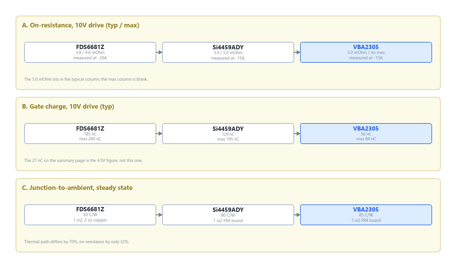
Figure 1. The same three measurements across the three parts. On-resistance at a 10V drive: 3.8 / 4.6 mOhm and 3.9 / 5.0 mOhm on the originals, 5.0 mOhm on the replacement with the maximum column left blank. Gate charge at 10V: 185, 129 and 56 nC. Junction-to-ambient at steady state: 50, 80 and 85 C/W, which puts the replacement 19.5C hotter than the FDS6681Z at 10A.
FAQ
Can the VBA2305 replace both the FDS6681Z and the Si4459ADY?
The package and pinout match, so both will solder down. The constraints differ. In a Si4459ADY position it drops in directly as long as the current stays under 10A. In an FDS6681Z position the 25V gate allowance has to be reduced to 20V first, and the cooling has to be recomputed at 85 C/W.
The summary pages say 5.0 mOhm against 4.6 mOhm. Why is the real gap larger?
The two numbers come from different columns. The 4.6 mOhm is a maximum, Si4459ADY's 5.0 mOhm is also a maximum, and the replacement's 5.0 mOhm is a typical with the maximum column blank. In the same column the replacement's typical has already passed the FDS6681Z maximum, and it is 28% above the Si4459ADY typical of 3.9 mOhm.
With no maximum published, what value should a volume design use?
Add 20% to the typical. That turns 5.0 mOhm into 6.0 mOhm, which is 30% above the FDS6681Z maximum of 4.6 mOhm and 20% above the Si4459ADY maximum of 5.0 mOhm. Record the assumption and the reason in the design file rather than copying the summary page.
How much lower is the gate charge?
It depends on the drive. At 10V the replacement is 56 nC, which is 30% of the FDS6681Z's 185 nC and 43% of the Si4459ADY's 129 nC. At 4.5V it is 27 nC, which is 26% and 44% of those two. The three summary-page numbers (27, 61 and 185) are taken at two different drives and cannot be divided directly.
What does lower gate charge buy?
Speed at the gate when the driver is weak. At 50 uA of charge-pump current, the time to reach 4.5V falls from 3.7 ms to 0.54 ms, so soft start is shorter and the device spends less time in the linear region during turn-on. On a board with a dedicated driver delivering amp-level peaks, it buys nothing.
Is -11A or -18A the current that can run continuously?
Neither is a direct answer. The -18A is at a 25C case with heat removed through the package; the -11A is 25C ambient for ten seconds only. On a board with no heatsink, working back from 85 C/W at a 60C ambient and a 150C junction gives about 12A using 25C resistance and about 11A using hot resistance.
What has to change in the cooling design when coming from the FDS6681Z?
Start by accepting a 19.5C higher junction at 10A. On a one-square-inch pad, the 85 C/W against 50 C/W gap cannot be closed with copper weight, so the options are lowering the current, adding a via array under the drain pad, or moving to a DFN8 5x6 part such as the VBQA2302.

Download PDF document
 Download now


