 中文
 English

VBQA2611 MOSFET Replacement for Si7461DP: Two Ordering Codes
 Back to previous page

The Si7461DP datasheet lists two ordering codes on its first page: -T1-E3 is lead-free, -T1-GE3 is lead-free and halogen-free. Page 2 holds a single electrical table that both codes share. A bill of materials that carries them as two separate parts will check the same die twice.
Both codes are 60V P-channel in a PowerPAK SO-8. Continuous drain current is -14.4A at a 25C ambient for 10 seconds, -8.6A at steady state. On-resistance at a 10V gate drive is 11.5 mOhm typical, 14.5 mOhm maximum.
The replacement is the VBQA2611, a 60V P-channel in DFN8 (5x6). On-resistance is 11 mOhm typical at 10V, 14 mOhm at 4.5V. Continuous current is -60A at a 25C case, footnoted as package limited, and the junction limit is 175C.
Three things need checking when the two sit side by side: the package name, the base of the current rating, and the fact that the replacement publishes no maximum on-resistance.
Four Places It Sits
| Position | How it is connected | Current range | What matters |
|---|---|---|---|
| Battery and circuit protection | In series between pack and load, source to the positive rail, gate pulled low by a protection IC | 3A to 12A | Steady-state thermal resistance, threshold ceiling |
| Load switch | Single high-side device, gate driven by a load-switch IC or an MCU through a level shifter | 1A to 10A | Gate charge, soft-start time |
| Motor drive | One direction or the low side of an H-bridge, gate pushed by a driver | Peaks up to 20A | Avalanche energy, pulsed current |
| Reverse polarity protection | In series at the input, body diode blocks a reversed supply | 5A to 15A | Body diode drop, steady-state thermal resistance |
The 60V rating leaves headroom on 12V, 24V and 48V rails. Reverse battery and the turn-off spike of an inductive load are what push against the rating, which is why these positions use 60V rather than 30V.
Two Ordering Codes, One Electrical Table
| Ordering code | Lead | Halogen |
|---|---|---|
| Si7461DP-T1-E3 | Lead-free | Not stated |
| Si7461DP-T1-GE3 | Lead-free | Halogen-free |
The suffix changes neither the electrical parameters nor the package and pinout. The only difference is the material declaration. Buy the -GE3 where halogen-free is required and take every other value from the same table.
Treat the two codes as one part during a replacement: one parameter check, one land pattern. Both codes stay in the bill of materials to cover two purchasing channels, not because there are two devices.
Package Name and Land Pattern
| Item | Si7461DP | VBQA2611 |
|---|---|---|
| Package name | PowerPAK SO-8 | DFN8 (5x6) |
| Body | 6.15 x 5.15 mm | 5 x 6 mm |
| Height | 1.07 mm | Not stated |
| Pins | 1-3 source, 4 gate, 5-8 drain, exposed pad to drain | Same |
The two names describe the same family of leadless packages, and the bodies differ by 0.15 mm in each direction. The name does not affect soldering. The land pattern does: the two recommended patterns differ in pad length and in how far the leads extend, so draw the narrower of the two and the other part still lands.
Use a reflow profile for leadless packages with a 260C peak. Hand soldering is not appropriate for this family; rework needs hot air.
Two Bases for the Current Rating
| Item | Si7461DP | VBQA2611 |
|---|---|---|
| Continuous current (25C ambient, 10 s) | -14.4A | Not listed |
| Continuous current (25C ambient, steady state) | -8.6A | Not listed |
| Continuous current (70C ambient, steady state) | -6.9A | Not listed |
| Continuous current (25C case) | Not listed | -60A, package limited |
| Continuous current (125C case) | Not listed | -36A |
| Pulsed current (100 us) | -60A | -100A |
The -14.4A on the original is a 25C ambient rating held for 10 seconds. The -60A on the replacement is a 25C case rating, and a footnote marks it as package limited. Put the two numbers side by side in a selection table and it reads as four times the capability, when it is really two different bases.
A case rating assumes heat leaves through the case. On a board with no heatsink, where copper does the work, only the ambient rating applies, and the replacement publishes no ambient current at all. It publishes a junction-to-ambient resistance of 68 C/W instead.
Working back from that: a 175C junction limit at a 25C ambient allows 2.21W. At 11 mOhm that is 14.2A. Raise the resistance by a factor of 1.5 for temperature, to 16.5 mOhm, and 11.6A is left.
The same arithmetic on the original: a 150C limit, a 60C ambient and 65 C/W maximum allows 1.38W. A 14.5 mOhm maximum raised to 20.3 mOhm gives 8.3A.
The two calculations do not use the same ambient, but the result lines up with the -8.6A the original publishes. Steady-state current lands between 8A and 10A for both, slightly higher on the replacement.
Thermal Resistance and the Junction Limit
| Item | Si7461DP | VBQA2611 |
|---|---|---|
| Junction-to-ambient, 10 s | 18 typ / 23 max | Not listed |
| Junction-to-ambient, steady state | 52 typ / 65 max | 68 |
| Junction-to-case, steady state | 1.0 typ / 1.3 max | 2.2 |
| Junction limit | 150C | 175C |
| Maximum dissipation | 5.4W at 25C ambient, 10 s / 1.9W steady | 68W at 25C case |
Both thermal resistances are worse on the replacement, 68 against 65 and 2.2 against 1.3. The junction limit moves the other way by 25C.
Combine them: at a 60C ambient, (175 - 60) / 68 = 1.69W against (150 - 60) / 65 = 1.38W. The replacement is allowed 22 percent more dissipation.
The thermal resistance alone does not settle this. The junction limit has to go into the same expression.
Test Current and Column for On-Resistance
| Item | Si7461DP | VBQA2611 |
|---|---|---|
| Test current at 10V drive | -14.4A | -10A |
| 10V drive, typical / maximum | 11.5 / 14.5 mOhm | 11.0 mOhm / not listed |
| Test current at 4.5V drive | -12.6A | -5A |
| 4.5V drive, typical / maximum | 15.0 / 19.0 mOhm | 14.0 mOhm / not listed |
| Junction at 125C, 10V drive | Curve only | 24.0 mOhm typical |
| Junction at 175C, 10V drive | Curve only | 36.0 mOhm typical |
Both resistance figures for the replacement sit in the typical column, with the maximum column empty. Both figures on the original carry a maximum guarantee.
Column against column: 11.0 against 11.5 is 4 percent lower at 10V; 14.0 against 15.0 is 7 percent lower at 4.5V. Against a maximum, the replacement has nothing to compare.
The test currents differ as well: -10A against -14.4A, and -5A against -12.6A. P-channel resistance rises a little with current, and the replacement is measured at the lower current, so the gap narrows once both are referred to the same current.
A production design has to take the worst case. With no maximum published, raise the typical by 20 percent to 13.2 mOhm and use that: 9 percent below the 14.5 mOhm maximum on the original.
Gate Charge and Avalanche Energy
| Item | Si7461DP | VBQA2611 |
|---|---|---|
| Gate charge at 10V, typical / maximum | 121 / 190 nC | 60 / 100 nC |
| Gate charge test current | -14.4A | -5A |
| Gate-source charge | 20 nC | 9.5 nC |
| Gate-drain charge | 32 nC | 19 nC |
| Gate resistance | 3 Ohm | 0.5 / 1.19 / 1.8 Ohm |
| Single-pulse avalanche energy | 125 mJ | 64.8 mJ |
| Avalanche current | 50A | 36A |
The two gate-charge numbers come from test currents that differ by a factor of 2.9, so they cannot simply be subtracted. Even taking the maximum of 100 nC, the replacement stays below the 121 nC typical of the original.
A load-switch IC often sources a few tens of microamps from its charge pump. At 50 uA, 190 nC takes 3.8 ms to reach 10V and 100 nC takes 2.0 ms. Soft-start time follows that number. Where a dedicated driver supplies amps of peak current, this item is worth nothing.
Avalanche energy is 48 percent lower on the replacement, and avalanche current is 36A against 50A. Motors, relays and long cables produce a spike at turn-off, and the replacement has less margin there: either clamp it or limit the current to 36A.
Pulsed current goes the other way, -100A against -60A. A single short pulse is not limited by the avalanche figure.
Threshold and 4.5V Drive
| Item | Si7461DP | VBQA2611 |
|---|---|---|
| Threshold, minimum / maximum | -1.0 / -3.0V | -1.5 / -3.5V |
| Gate-source rating | +/-20V | +/-30V |
| Overdrive at 4.5V drive | 1.5V | 1.0V |
| On-resistance at 2.5V drive | Not listed | Not listed |
The threshold ceiling moves from -3.0V to -3.5V. At a 4.5V drive the overdrive above that ceiling drops from 1.5V to 1.0V, so this drive level is tighter on the replacement. Neither datasheet lists on-resistance at 2.5V, so the low end has to be measured.
The gate rating moves from +/-20V to +/-30V, which is looser on the replacement. On a 24V rail, pulling the gate of a high-side P-channel to ground puts -24V across gate and source: the original is over its rating and needs a Zener clamp or a series divider, while the replacement stays inside.
On a 12V rail both are safe and this item makes no difference.
Three Ways to Proceed
The first: a 24V rail, gate taken straight to ground, current under 8A. Replace directly. The original needed a clamp that the +/-30V rating makes unnecessary, and the thermal calculation is redone at 68 C/W.
The second: a 12V rail, current under 10A, gate driven or clamped. Replace directly. Gate charge halves, and switching loss follows it down.
The third: above 12A, or a turn-off spike large enough that avalanche margin matters. This part is not the answer. The VBQA2606 shares the package and the voltage rating at 6 mOhm and -80A, at twice the gate charge.
Full Parameter Comparison
| Parameter | Si7461DP | VBQA2611 |
|---|---|---|
| Package | PowerPAK SO-8 | DFN8 (5x6) |
| Channel | P | P |
| VDS | -60V | -60V |
| VGS | +/-20V | +/-30V |
| Threshold, min / max | -1.0 / -3.0V | -1.5 / -3.5V |
| RDS(on) at 10V, typ / max | 11.5 / 14.5 mOhm | 11.0 / not listed |
| RDS(on) at 4.5V, typ / max | 15.0 / 19.0 mOhm | 14.0 / not listed |
| Continuous current, 25C ambient | -14.4A (10 s) / -8.6A (steady) | Not listed |
| Continuous current, 25C case | Not listed | -60A (package limited) |
| Continuous current, 125C case | Not listed | -36A |
| Pulsed current | -60A | -100A |
| Body diode drop, typ / max | -0.8 / -1.2V | -0.80 / -1.2V |
| Gate charge at 10V, typ / max | 121 / 190 nC | 60 / 100 nC |
| Gate-source charge | 20 nC | 9.5 nC |
| Gate-drain charge | 32 nC | 19 nC |
| Gate resistance | 3 Ohm | 0.5 / 1.19 / 1.8 Ohm |
| Input capacitance | Curve only | 4000 pF |
| Output capacitance | Curve only | 310 typ / 450 max pF |
| Reverse transfer capacitance | Curve only | 200 typ / 275 max pF |
| Transconductance | 31 S | 26 S |
| Junction-to-ambient, steady state | 52 typ / 65 max C/W | 68 C/W |
| Junction-to-case, steady state | 1.0 typ / 1.3 max C/W | 2.2 C/W |
| Avalanche energy | 125 mJ | 64.8 mJ |
| Junction range | -55 to 150C | -55 to 175C |
Other Options at 60V
The VBQA2606 is a 60V P-channel in the same package: 6.0 mOhm at 10V, 7.5 mOhm at 4.5V, -80A at a 25C case and -240A pulsed. It is a little over half the resistance, twice the gate charge, and the same 64.8 mJ of avalanche energy. Above 12A this is the one to take, and the land pattern does not change.
The VBA2305 is a 30V P-channel in a SOP-8, 5.0 mOhm and -18A. Half the voltage rating, so it only makes sense on rails below 30V, and the land pattern has to be redrawn.
Staying with the original is also a choice. Between 8A and 10A both devices cover the load switch, and what separates them is gate charge and gate rating.
Checks Before Replacing
- Land pattern: the two recommended patterns differ; draw the narrower one. The exposed pad is the drain, and the via array has to sit inside it.
- Current: the -60A on the replacement is a case rating and package limited. With no heatsink, work back from 68 C/W and expect about 10A at steady state.
- Resistance: no maximum is published. Raise the typical by 20 percent to 13.2 mOhm for the design value.
- Avalanche: 64.8 mJ and 36A, half of the original. Clamp inductive loads or limit current to 36A.
- Gate: the replacement takes +/-30V, so a 24V rail can pull the gate to ground directly. At a 4.5V drive the overdrive is only 1.0V, and the low end has to be measured.
- Product page: the parameter table there says -50A, +/-20V and a -2.5V threshold, while the datasheet says -60A, +/-30V and -1.5 to -3.5V. Take the datasheet and confirm with the supplier before ordering.
- Ordering codes: -T1-E3 and -T1-GE3 are one die with different halogen declarations, not two devices.
- Pinout: 1-3 source, 4 gate, 5-8 drain, exposed pad to drain, identical on both parts.
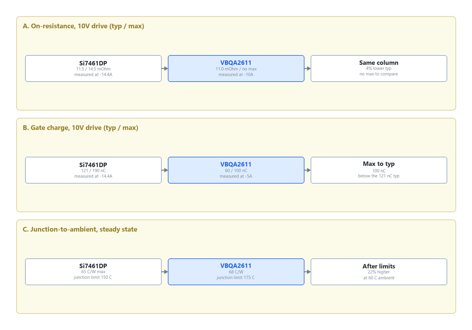
Figure 1. The same three measurements across the two parts. On-resistance at a 10V drive: 11.5 mOhm typical and 14.5 mOhm maximum on the original, 11.0 mOhm typical on the replacement with the maximum column left blank. Gate charge: 121 / 190 nC against 60 / 100 nC. Junction-to-ambient at steady state: 65 C/W maximum against 68, with the replacement carrying a 175C junction limit instead of 150C.
FAQ
Are Si7461DP-T1-E3 and -T1-GE3 two different devices?
No. The datasheet lists both codes under ordering information: -E3 is lead-free, -GE3 is lead-free and halogen-free. They share one electrical table, one package and one pinout, so a replacement checks the part once.
The replacement claims -60A against -14.4A. Is it four times stronger?
The bases differ. -14.4A is a 25C ambient rating held for 10 seconds; -60A is a 25C case rating marked package limited. Working back from 68 C/W, a 25C ambient supports about 11.6A at steady state, the same order as the 8.6A of the original.
The package names differ. Can it be soldered in place?
PowerPAK SO-8 and DFN8 (5x6) differ by 0.15 mm in each direction, and the pinout matches. It can be soldered directly, but draw the narrower of the two land patterns; the exposed pad length is where they differ most.
Only a typical resistance is published. What value goes into the design?
Raise the typical by 20 percent. 11.0 mOhm becomes 13.2 mOhm, which is 9 percent below the 14.5 mOhm maximum on the original. Record that derivation in the design file.
Can the gate be pulled straight to ground on a 24V rail?
Yes. The original is rated +/-20V, so -24V already exceeds it and needs a clamp; the replacement is rated +/-30V and stays inside. This is one of the few places where it is the looser part.
Where does the lower avalanche energy matter?
Motors, relays, long cables and hot-swap inputs, wherever a turn-off spike appears. The replacement is 64.8 mJ and 36A against 125 mJ and 50A, so clamp the spike or limit the current to 36A.
Is this part still the choice above 12A?
No. The VBQA2606 in the same package and voltage class is 6.0 mOhm and -80A with the same land pattern, at twice the gate charge.

Download PDF document
 Download now


