 中文
 English

VBM1803 MOSFET Replacement for CSD19505KCS: 80V, 195A, TO-220
 Back to previous page
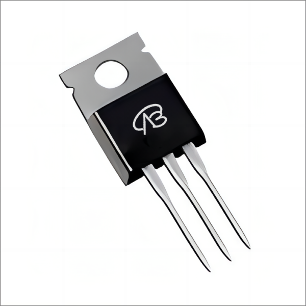
The CSD19505KCS is an 80V single N-channel MOSFET in TO-220. On-resistance is 2.6 mOhm typical and 3.1 mOhm maximum at 10V of drive, measured at 100A. Continuous drain current is 208A at a 25C case, 150A as a package limit, and junction-to-case thermal resistance is 0.5C/W. It shows up in these positions: secondary-side synchronous rectification on a 48V output, the DC-DC stage of a telecom supply, the battery-side switch in a power tool, one leg of a low-voltage servo bridge. All four carry high current and conduct for long stretches, so the first numbers read are on-resistance, thermal resistance and avalanche capability.
The replacement candidate is VBM1803, same package and same voltage class: 80V, 2.8 mOhm at 10V of drive, 195A at a 25C case, 0.4C/W junction-to-case. Both are trench devices with an identical pinout, so the part drops in.
The differences sit in four places: on-resistance is published as a typical value only, the threshold ceiling is 0.8V higher, avalanche energy is less than half, and the current ratings are stated on a different basis. None of the four affects whether the part can be soldered in. All four affect whether the original margin survives the swap.
Where the part sits
| Position | How it is connected | Current range | What is watched |
|---|---|---|---|
| Secondary-side sync rectification on a 48V output | Two devices across the secondary, gates from an isolated driver | 60A to 120A | Body-diode reverse recovery, dead-time loss |
| DC-DC stage of a telecom supply | Low side of a half or full bridge, source at power ground | 50A to 150A | Conduction loss, gate charge |
| Battery-side switch in a power tool | In the negative return, gate driven by the protection board | 30A to 80A | Short-circuit withstand, avalanche |
| One leg of a low-voltage servo bridge | Upper and lower device of one leg, isolated gate drive | 20A to 80A | Avalanche energy, dv/dt immunity |
The first two conduct continuously. The last two switch inductive loads. That split decides how much weight each of the four differences carries: continuous conduction is about on-resistance and thermal resistance, switching is about threshold, charge and avalanche.
Two readings of on-resistance
Both data sheets put the number on one line, but the conditions behind that line differ:
| Item | CSD19505KCS | VBM1803 |
|---|---|---|
| Test current | 100A | 30A |
| Typical at 10V of drive | 2.6 mOhm | 2.8 mOhm |
| Maximum at 10V of drive | 3.1 mOhm | not published |
| Intermediate point | 6V drive: 2.9 typ / 3.8 max | 7.5V drive: 3.0 typ, no max |
Reading 2.6 against 2.8 produces the conclusion that the replacement sits one step worse on resistance. That conclusion does not hold, because the test currents differ by a factor of 3.3. Page 3 of the replacement data sheet carries an on-resistance against drain current curve running from 0 to 100A: the 10V trace goes from 2.50 mOhm at zero to 2.60 mOhm at 100A, a rise of 0.10 mOhm across the whole span. Converted to the 100A condition, the typical value is 2.6 mOhm, level with the original.
What is missing is not the typical value but the maximum. The 3.1 mOhm of the original is a guaranteed limit that no unit in a shipment exceeds. The replacement fills the typical column and leaves the maximum empty, while the front-page product summary prints that typical number under a maximum heading. Designing to a typical value treats an expectation as a ceiling.
The consequence is arithmetic. At 100A of continuous conduction, 2.6 mOhm dissipates 26W and 3.1 mOhm dissipates 31W, a 5W spread. With 0.4C/W junction-to-case, that is 12.5C of case temperature. A heatsink sized with 20 percent margin absorbs the spread. One sized without margin goes straight to the limit.
The threshold window
| Item | CSD19505KCS | VBM1803 |
|---|---|---|
| Minimum | 2.2V | 2.0V |
| Typical | 2.6V | not published |
| Maximum | 3.2V | 4.0V |
At 10V of drive this row does nothing. Both parts sit more than 6V above threshold and the transconductance is saturated. The row matters at 5V and 4.5V of drive: worst-case overdrive is 1.8V on the original and 1.0V on the replacement. At 1V of overdrive the channel is not fully enhanced, on-resistance rises, and neither data sheet gives an on-resistance figure at 4.5V that can be used to quantify the rise.
The 4.5V on-resistance for the replacement appears only on the product page, written as 4 mOhm, and it comes from a curve rather than a specification table. That number cannot serve as a guaranteed value.
Where the board already drives the gate at 10V, this row can be closed. Where the gate is pulled up from an MCU through a transistor, or driven from 5V logic, the drive has to be raised before the swap, or a device with a lower threshold ceiling has to be selected.
Avalanche energy and inductive loads
| Item | CSD19505KCS | VBM1803 |
|---|---|---|
| Single-pulse avalanche energy | 510 mJ | 245 mJ |
| Avalanche current | 101A | 70A |
| Inductance | 0.1 mH | 0.1 mH |
| Gate resistance in the test | 25 Ohm | not stated |
The two energy figures differ by more than a factor of two, but the difference comes from the permitted avalanche current, not from ruggedness. Single-pulse energy is 0.5 x L x I squared: 0.1 mH with 101A gives 510 mJ, with 70A gives 245 mJ, and each data sheet is internally consistent. The number to compare is therefore 101A against 70A, a 30 percent gap.
That gap lands on power tools and motor drives. Windings, relay coils and long cable runs push stored energy back into the drain at turn-off, and the device absorbs it in avalanche. The original permits 101A of avalanche current, the replacement 70A; beyond that the device enters second breakdown. Substituting load inductance, turn-off current and operating temperature into 0.5 x L x I squared and reading this row is more direct than comparing the energy figures.
In telecom supplies and synchronous rectification the drain is clamped to the output plus a diode drop, so avalanche is rarely reached and this row can be closed.
Three ways to state current
The same class of device, rated three different ways:
| Item | CSD19505KCS | VBM1803 |
|---|---|---|
| Package limit | 150A | not listed separately |
| Silicon limit, 25C case | 208A | 195A |
| Silicon limit, 100C case | 147A | 70C case: 120A |
| Pulsed current, 100 us | 400A | 600A |
| Power dissipation at 25C | 300W | 375W |
The original separates the package limit from the silicon limit onto two lines, 150A and 208A, so the two cannot be confused. The replacement gives one pair, 195A and 120A, and attaches a package-limit footnote to the current row. The same TO-220 package therefore carries two different package limits, 45A apart. That has to be settled at selection: is 195A silicon or package.
Which line governs depends on case temperature. With a heatsink holding the case below 80C the silicon limit dominates. Under natural convection, or with the case above 90C, both lines fall and the smaller one governs. The original gives 147A at a 100C case; the replacement does not give that point, so interpolation between 25C and 70C has to be used, and that interpolation is uncertain across 80C to 100C.
Pulsed current runs the other way: 600A against 400A. Where short-circuit protection acts in the 10 us range, that row carries weight.
Full specification comparison
Both parts, specification values only:
| Parameter | CSD19505KCS | VBM1803 | Note |
|---|---|---|---|
| Drain-source voltage | 80V | 80V | Same class |
| Gate-source voltage | +/-20V | +/-20V | Same |
| On-resistance at 10V | 2.6 typ / 3.1 max | 2.8 typ / no max | 100A vs 30A |
| Threshold voltage | 2.2 / 2.6 / 3.2V | 2.0 / none / 4.0V | Ceiling 0.8V higher |
| Gate charge at 10V | 76 nC typ | 94 typ / 141 max | 100A vs 20A |
| Gate-drain charge | 11 nC | 10 nC | Level |
| Input capacitance | 6090 typ | 7910 typ | At 40V |
| Output capacitance | 1600 typ | 3250 typ | At 40V |
| Reverse transfer capacitance | 26 typ | 348 typ | At 40V, 13x |
| Gate resistance | 1.4 typ / 2.8 max | 0.28 / 1.4 / 2.8 | Same |
| Body-diode forward voltage | 0.9 typ / 1.1 max | 0.8 typ / 1.5 max | 100A vs 10A |
| Reverse recovery charge | 400 nC typ | 315 typ / 475 max | 100A vs 34A |
| Reverse recovery time | 88 ns typ | 126 typ / 190 max | Same conditions |
| Junction-to-case | 0.5C/W | 0.4C/W | 20 percent lower |
| Junction-to-ambient | 62C/W | 40C/W | Board conditions differ |
| Avalanche energy | 510 mJ | 245 mJ | 101A vs 70A |
| Junction temperature | -55 to 175C | -55 to 175C | Same |
Thermal resistance is better on the replacement, on both rows. The junction-to-ambient row cannot be compared directly because neither data sheet states the board conditions in full, so a heatsink design uses only the junction-to-case row.
The charge rows need direction. The replacement carries 24 percent more gate charge, 30 percent more input capacitance and twice the output capacitance, all pointing to a heavier drive load. At 20kHz and 10V of drive, 94 nC and 76 nC work out to 18.8 mW and 15.2 mW of drive loss, a 3.6 mW gap that is not decisive at that frequency. Above 100kHz the row needs its own calculation.
The 13x gap in reverse transfer capacitance is the largest single difference between the two data sheets. Yet the gate-drain charge on the same sheet is 10 nC, level with the original, which says the two numbers describe different voltage spans: the capacitance is a single point at 40V, the charge is an integral from zero to 40V. Displacement current during dv/dt is estimated from gate-drain charge; steady-state parasitic estimates use reverse transfer capacitance. The two serve different purposes and cannot stand in for each other.
Other options at 80V
Where the current requirement sits below 75A and a smaller package is wanted, VBE1806 is 80V in TO252, 5 mOhm at 10V of drive, 75A. The voltage class matches; package and thermal resistance do not, so the two cannot be exchanged without recalculating the heatsink.
Where the voltage has to reach 100V, VBGQF1101N is DFN8 (3x3), 100V, 50A, 10.5 mOhm at 10V of drive. Moving from TO-220 to a surface-mount package changes the thermal path from a heatsink to copper on the board, which is a larger change than swapping the device.
This article covers drop-in replacement at the same package and voltage. The two parts above serve only as current and voltage reference points across packages.
Checks before substitution
| Check | How to look | Consequence if it fails |
|---|---|---|
| Gate drive level | Measure the actual high level at the gate, 10V or 5V | At 5V the worst-case overdrive is 1.0V and resistance rises |
| Thermal margin | Loss from the typical resistance plus 20 percent, then case temperature | No guaranteed maximum on the replacement, so thin margin overheats |
| Inductive energy | 0.5 x L x I squared against 245 mJ | Beyond it the device avalanches; the replacement permits 70A |
| Operating case temperature | Measured or simulated heatsink temperature | The replacement gives 25C and 70C only, nothing above 80C |
| Short-circuit timing | Protection response time against the 600A pulse rating | Protection slower than 100 us means continuous current governs |
| Package and pinout | TO-220, pin 1 gate, pin 2 drain, pin 3 source | Identical, drops in |
| Pad and mounting hole | Hole diameter and heatsink screw position | Different means a mechanical change |
Package and pinout are identical, so no board change is needed. The real work sits in the gate drive and thermal margin rows, both of which are circuit and mechanical decisions.
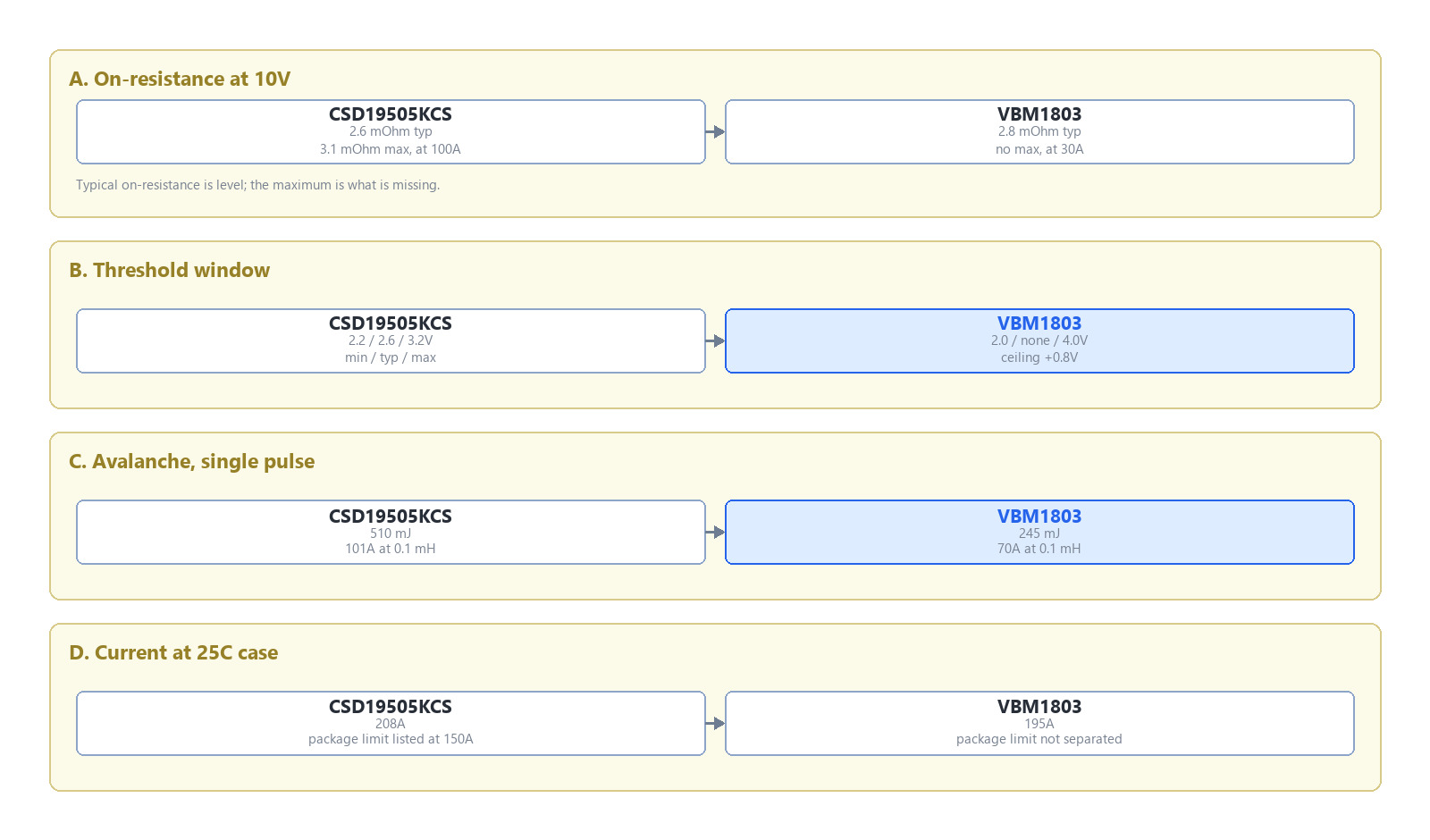
Figure 1. Four differences between the VBM1803 and the CSD19505KCS. On-resistance at a 10V gate drive, measured at 100A on the original (2.6 mOhm typical, 3.1 mOhm maximum) and at 30A on the replacement (2.8 mOhm typical, no maximum published). The threshold ceiling moves from 3.2V to 4.0V. Single-pulse avalanche energy falls from 510 mJ to 245 mJ. Continuous current at a 25C case goes from 208A to 195A, while the package limit on the original is listed separately at 150A.
FAQ
Can the VBM1803 replace the CSD19505KCS directly?
Package, pinout and voltage class match, so it drops in. Confirm three things first: the board drives the gate at 10V, the heatsink carries at least 20 percent margin, and the load is not a large inductance switched off directly. With all three satisfied the swap is direct.
Which part has the lower on-resistance?
Level, when compared on the same conditions. The 2.6 mOhm of the original is measured at 100A, the 2.8 mOhm of the replacement at 30A. The replacement's on-resistance against current curve runs from 2.50 mOhm at zero to 2.60 mOhm at 100A on the 10V trace, so at 100A it is also 2.6 mOhm. The difference is in the maximum: the original guarantees 3.1 mOhm, the replacement publishes none.
The replacement has no maximum on-resistance. What value goes into the design?
The typical value plus margin. Batch design normally works from the maximum, which is absent here, so 2.6 mOhm is raised 20 percent to 3.1 mOhm as the design value, level with the original. The reasoning should be written into the design record.
Can it be driven at 4.5V?
Not recommended. The threshold ceiling is 4.0V, so worst-case overdrive at 4.5V is 0.5V and the device never fully enhances. The 4 mOhm on the product page comes from a curve, not from a guaranteed table entry.
Avalanche energy is less than half. Which applications care?
Motor drives, power tools, relays and long cable runs, where turn-off pushes inductive energy back into the drain. In synchronous rectification and telecom supplies the drain is clamped and avalanche is rarely reached, so the row can be closed. Compute the load energy as 0.5 x L x I squared and compare against 245 mJ.
Is the package limit 150A or 195A?
The original lists the package limit separately at 150A with a silicon limit of 208A. The replacement gives 195A and footnotes the current row as package limited. Two package limits for the same TO-220 means taking the smaller one and confirming the basis of 195A with the supplier.
Junction-to-ambient is 40C/W against 62C/W. Why not use that directly?
Neither data sheet states the test board in full: copper area, layer count and whether a heatsink was fitted all differ. Estimating 40C/W for a board cooled only by copper runs optimistic. With a heatsink, only the junction-to-case row is used, and both parts publish it.

Download PDF document
 Download now


