 中文
 English

NTTS2P02R2 P-Channel MOSFET Replacement: Heat Sets the Current
 Back to previous page

The NTTS2P02R2 is a single P-channel MOSFET in the Micro8 package, eight leads on a 3 by 3 mm body, rated -20V with 90 milliohms at 4.5V gate drive and -2.4A at 25C ambient. It sits in battery management inside portable equipment: the charge and discharge path of a single lithium cell, the switch between battery and USB input, and the load switch for a PCMCIA card or a small vibration motor. Current in these positions runs from 1A to 2A, the gate is static, and the board provides only a small copper area, so heat leaves through the eight leads.
The manufacturer lists this order code as obsolete. The lead-free version, NTTS2P02R2G, uses the same die with a G appended to the code, and it is obsolete as well. The two differ only in lead finish, and their electrical specifications are identical.
For a device swap, VBA8338 comes in the same package with the same pinout: -30V, 25 milliohms at 4.5V drive, and -6.0A at 25C. Its on-resistance is 28% of the original, and its input capacitance is 2.9 times higher. Those two figures move in opposite directions, and that decides which positions take the swap directly and which need the switching loss calculated first.
Where the part sits
| Position | How it is wired | What it has to do |
|---|---|---|
| Charge and discharge path of one lithium cell | Source toward the system, gate driven by a control pin or a charger IC | Conducts continuously, and the drop comes straight out of run time |
| Switch between battery and USB input | Two devices back to back, gates cross-controlled | Thresholds must match, and no body diode may conduct backwards |
| Load switch in portable equipment | Source toward the load, gate pulled down by an MCU | Low current, so thermal resistance sets the rise |
| Isolation on a 3.3V or 5V rail | In series with the rail, gate on the logic level | Must stay low resistance at low gate drive |
What these positions share is modest current and a gate that does not move. In this class of application the deciding column is not the current rating but the thermal path: at the same 2A, a generous copper area and a minimal one differ by tens of degrees.
Rating and thermal resistance
The datasheet says -2.4A, and that number rests on two conditions: minimum FR-4 board, steady state, with a junction-to-ambient resistance of 160C/W. Move the same device to a 2-inch square board with 2-ounce copper and the resistance falls to 88C/W while the rating rises to -3.25A. One order code, two ratings, and the whole difference is how much copper the board gives it.
Using 160C/W and 90 milliohms, with the junction held below 150C:
| Continuous current | Loss | Rise | Junction at 25C ambient | Junction at 85C ambient |
|---|---|---|---|---|
| 0.5A | 0.023W | 3.6C | 29C | 89C |
| 1.0A | 0.090W | 14.4C | 39C | 99C |
| 1.5A | 0.203W | 32.4C | 57C | 117C |
| 2.0A | 0.360W | 57.6C | 83C | 143C |
| 2.4A | 0.518W | 82.9C | 108C | 168C |
The published -2.4A holds at 25C ambient; in an 85C enclosure the junction passes the limit by 18C. At 85C ambient the device can carry 2.1A, which is (150 minus 85) divided by 160 for allowable dissipation, then divided by 90 milliohms and square-rooted.
The replacement moves two figures in the same direction. On-resistance falls from 90 to 25 milliohms and steady-state thermal resistance from 160 to 95C/W:
| Continuous current | Replacement loss | Replacement rise | Junction at 85C ambient |
|---|---|---|---|
| 1.0A | 0.025W | 2.4C | 87C |
| 2.0A | 0.100W | 9.5C | 95C |
| 2.4A | 0.144W | 13.7C | 99C |
| 5.0A | 0.625W | 59.4C | 144C |
At 85C ambient the replacement tops out at 5.2A, using the same arithmetic with 95C/W and 25 milliohms. That is 2.1A against 5.2A, and the gap comes from resistance and thermal resistance falling together. A position that used to run against its limit ends up with room to spare.
Comparison with VBA8338
The full comparison, using datasheet values only:
| Parameter | NTTS2P02R2 | VBA8338 | Change |
|---|---|---|---|
| Package | Micro8 (3x3 mm) | MSOP8 (3x3 mm) | Same pinout |
| VDSS | -20V | -30V | One step higher |
| VGS limit | plus or minus 8.0V | plus or minus 20V | Wider |
| VGS(th) | -0.5V to -1.4V | -1.7V max | Replacement higher |
| RDS(on) at -4.5V | 90 milliohms max (-2.4A) | 25 milliohms max (-5.6A) | 72% lower |
| RDS(on) at -2.7V | 130 milliohms max (-1.2A) | Not specified | - |
| RDS(on) at -2.5V | 110 milliohms typical (-1.2A) | Not specified | - |
| ID at TA 25C | -2.4A | -6.0A | 1.5 times higher |
| ID at TA 70C | -1.92A | -4.6A | Higher |
| Qg typical / max at -4.5V | 10nC / 18nC | 13nC / 20nC | 30% higher typical |
| Ciss | 550pF | 1600pF | 2.9 times higher |
| RthJA | 160C/W (minimum board) | 50C/W (t up to 10 s), 95C/W steady state | Better |
| PD at TA 25C | 0.78W | 2.5W | 2.2 times higher |
| VSD | -1.0V max (IS = -2.4A) | -1.2V max | Slightly worse |
| Status | Obsolete | In production | - |
The only column that gets worse is capacitance. Everything else, including voltage rating, gate limit, current, thermal resistance and dissipation, moves the same way. Every other device in this group forces at least one concession; this one does not, but the cost lands in the switching transient rather than in any static figure. The ranking across the group was laid out earlier in the six-part comparison.
Input capacitance and gate charge
The original gives 550pF input capacitance and 10nC typical gate charge; the replacement gives 1600pF and 13nC typical, both at 4.5V drive.
Start with drive loss, which scales as Qg times drive amplitude times frequency. At 4.5V drive and 100kHz the original dissipates 4.5 microwatts and the replacement 5.9 microwatts, a difference of 1.4 microwatts. That magnitude does not matter in any application.
The real effect is in the transition. The gate time constant is gate resistance times input capacitance, so at the same 6-ohm resistor it goes from 3.3ns to 9.6ns and the edge stretches by roughly 2.9 times. Switching loss is proportional to edge time, so put what conduction saves against what switching costs:
| Switching frequency | Conduction saving (2A continuous) | Switching penalty (12V bus) | Net |
|---|---|---|---|
| 100kHz | 260mW | about 70mW | plus 190mW |
| 300kHz | 260mW | about 210mW | plus 50mW |
| 500kHz | 260mW | about 350mW | minus 90mW |
The switching penalty is extrapolated from datasheet switching times and the capacitance ratio; the board waveform governs the real figure. What the table does is draw a line: below 200kHz the larger capacitance does not change the conclusion, and above 500kHz the penalty eats the conduction saving, so the swap stops being a clear win.
One case is easy to miss. At light load, conduction loss falls with the square of current while switching loss depends only on frequency, so the ratio between them flips. A position that runs 0.5A continuously at 400kHz can end up hotter after the swap than before it.
Low-voltage drive and threshold
The original is a logic-level device with a threshold from -0.5V to -1.4V, and its datasheet gives on-resistance at 4.5V, 2.7V and 2.5V drive. At 2.5V gate drive and 1.2A it is 110 milliohms typical, a figure that matters where a single lithium cell drives the gate directly.
A related part at the same -20V rating, the IRF7663, runs the opposite way: its gate limit is only plus or minus 12V, so the drive voltage has to be checked before anything else. For the device in hand, the replacement's threshold tops out at -1.7V, leaving 0.8V of overdrive at 2.5V drive, and its datasheet carries no figure for that drive level. Extrapolating from the 25 milliohms at 4.5V is not valid, because the channel is not fully enhanced and the real resistance is several times higher.
Two cases follow. With the gate driven from a 3.3V or 5V logic pin, the replacement is fine. With the gate tied to a 2.5V reference or to a lithium cell, measure first. Above 3.0V cell voltage the overdrive exceeds 1.3V and the replacement turns on fully; below 3.0V the replacement sits in a region the datasheet does not cover, while the original still has 2.7V-drive data to work from.
Using the gate voltage headroom
The original has an 8.0V gate limit and the replacement has 20V. That column widens, but a wider limit does not mean the drive amplitude can be raised.
A part with an 8V limit that has run in a production design for years is itself a measurement: the gate node, ringing included, never exceeded 8V. Swapping to 20V only removes that constraint. It does nothing for edge rate, dv/dt or immunity to spurious turn-on, all three of which are set by the gate resistor and the pull-down, never by the voltage rating. Raising the drive to 12V changes switching loss, EMI and body-diode recovery together, and the datasheet will not mention any of it.
One place does change. In a 12V system the original needs a divider before the gate and the replacement can be driven directly. Driving it directly speeds up the switching, which changes dv/dt and radiated emissions; that section has to be measured again rather than assumed better.
When the swap pays off
| Situation | Conclusion | Reason |
|---|---|---|
| Up to 2A continuous, switching below 200kHz | Swap directly | Resistance down 72%, thermal resistance down 41%, capacitance irrelevant |
| Running 2.4A in an 85C enclosure | Swap, and sooner | The original is down to 2.1A at 85C; the replacement has 5.2A |
| Switching above 500kHz | Calculate switching loss first | Capacitance is 2.9 times higher and the net can turn negative |
| Under 0.5A continuous at high frequency | Keep the original, or pick another part | Conduction loss was never the problem, so only the capacitance penalty remains |
| Gate driven from a 2.5V reference | Measure before deciding | Threshold is -1.7V, leaving under 1V of overdrive at 2.5V |
| Bus above 16V | Swap, with more to gain | The original reaches only 16V on an 80% derating; the replacement reaches 24V |
| 12V system with a gate divider | Keep the divider | Removing it changes switching speed and EMI |
The 12V case deserves a sentence of its own. Some boards drop 12V through a divider to keep the gate under 8V, and once the gate limit is 20V that divider looks redundant. Removing it raises the switching speed by a step, and both dv/dt and EMI have to be re-measured. Keeping the divider costs nothing in any static parameter.
Checks before the change
What is the continuous current on this path? Under 2A the swap is direct; at 2.4A continuous the replacement is the safer part.
What is the switching frequency? Below 200kHz capacitance does not matter; above 500kHz work out the net gain from the real waveform.
What is the highest ambient inside the enclosure? The published -2.4A is a 25C figure, and at 85C the original carries only 2.1A.
Which board was the rating measured on? The two ratings differ by 35%, and a minimum board is not a 2-inch board.
What drives the gate? A 3.3V or 5V logic pin is fine; a 2.5V reference needs a measurement first.
Is there a divider in a 12V system? Keep it, because removing it changes switching speed.
Is there an N-channel part in the same package? P and N devices share the 3x3 mm eight-lead footprint, and a wrong reel does not stop the placement machine.
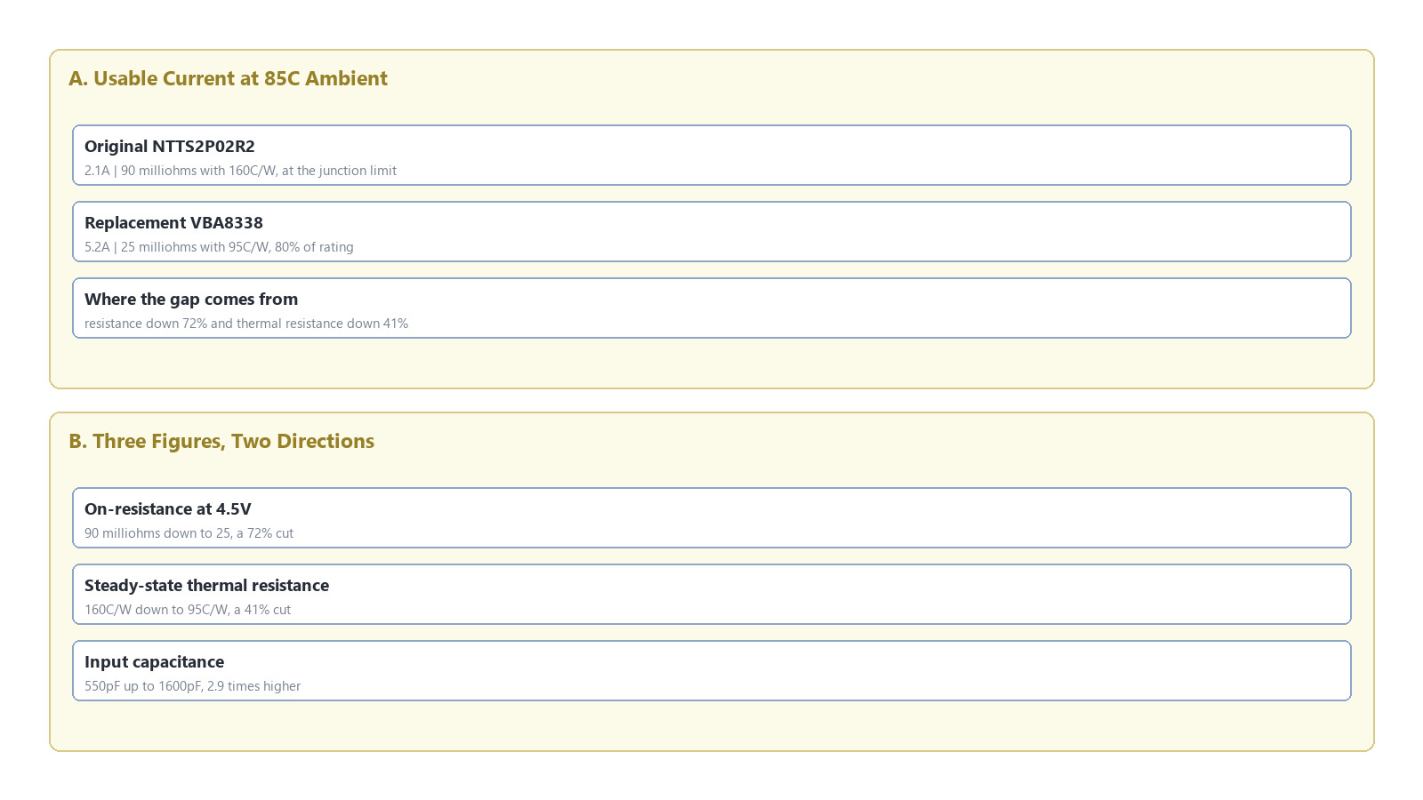
Figure 1: Conduction loss and junction temperature for the NTTS2P02R2 and VBA8338 in the same position. Resistance falls from 90 to 25 milliohms and steady-state thermal resistance from 160 to 95C/W, lifting usable current at 85C ambient from 2.1A to 5.2A.
Questions
Is the NTTS2P02R2 obsolete? Yes. The lead-free version NTTS2P02R2G uses the same die with a G appended to the code, and it is obsolete as well; the two differ only in lead finish.
Why does the NTTS2P02R2 have two current ratings? The datasheet gives two sets, one for a minimum FR-4 board at steady state with 160C/W and -2.4A, and one for a 2-inch square board with 2-ounce copper at 88C/W and -3.25A. Same order code, different copper.
Can it still carry 2.4A at 85C ambient? No. Allowable dissipation is (150 minus 85) divided by 160, or 0.41W, which over 90 milliohms gives 2.1A. Carrying 2.4A at 85C requires a thermal resistance below 140C/W, which means more copper.
How much current can VBA8338 carry in the same position? 5.2A at 85C ambient, capped by its -6.0A board rating; -6.0A at 25C. For a position that ran at 2A this is surplus capability, and the benefit shows up as lower rise and longer life.
Does the 2.9 times higher input capacitance cause trouble? Below 200kHz switching it barely matters. Above 500kHz the switching penalty is comparable to the conduction saving and has to be recalculated from the board waveform; a light-load position at 0.5A and high frequency can end up hotter than before.
The gate limit went from 8V to 20V, so can the drive voltage go up? Not advisable. The 8V limit was validated in production, and driving at 12V only changes edge rate and EMI without lowering on-resistance.

Download PDF document
 Download now


