 中文
 English

NTTS2P03R2 P-Channel MOSFET Replacement: -30V Power Path at 24V
 Back to previous page

NTTS2P03R2 is a single P-channel MOSFET in Micro8, 3 x 3 mm with eight leads, -30V, 63 mOhm typical at -10V gate drive, rated -2.48A at 25C ambient. It sits in places a -20V part cannot cover: the input switch behind a 24V adapter, the 8.4V charge and discharge path of a two-cell pack, load switching on a 12V rail, and PCMCIA card power gating in older portable equipment. Bus voltage runs from 12V to 24V and has to survive adapter plug-in ringing, which leaves no margin on a -20V device.
The manufacturer lists the part as obsolete. The lead-free version NTTS2P03R2G uses the same die and carries the same status. The difference between the two is lead finish only.
VBA8338 is a same-package, same-footprint alternative in the same voltage class: -30V, 18 mOhm at -10V gate drive, -6.0A at 25C ambient. The voltage rating does not change. What changes is on-resistance, thermal resistance and gate drive level. The failure mode in this class is not whether the part fits. It is which rating the design was built against: the datasheet carries four sets of them and the product page quotes the loosest.
Where the part sits
| Position | Connection | Why the -30V class |
|---|---|---|
| 24V adapter input switch | Source to system, gate driven by adapter detect | 24V plus plug-in ringing approaches 30V |
| Two-cell pack charge and discharge | Back-to-back pair, cross-coupled gates | 8.4V at full charge, tight on a -20V part at temperature |
| 12V rail load switch | In series with the rail, gate pulled low by the MCU | 12V plus inductive flyback, spikes past 20V |
| PCMCIA card and legacy portables | Gate driven by the card detect signal | One part covering both the 5V and 12V branches |
The common thread is a bus above 12V, current between 1A and 2A, and conduction that is long or continuous. The selection decision lands on the thermal path and the rating basis, not on the headline current number.
Where four ratings come from
One datasheet, four sets of ratings, set by board and by time:
| Test condition | Thermal resistance | PD at 25C | ID at 25C | ID at 70C |
|---|---|---|---|---|
| Minimum FR-4 board, t <= 10 s | 160C/W | 0.78W | -2.48A | -1.98A |
| 2-inch square, 2 oz copper, t <= 10 s | 70C/W | 1.78W | -3.75A | -3.0A |
| Minimum FR-4 board, steady state | 210C/W | 0.60W | -2.10A | -1.67A |
| 2-inch square, 2 oz copper, steady state | 100C/W | 1.25W | -3.02A | -2.42A |
The -2.48A on the product page and in the headline is the first row: minimum board, ten seconds. Put the same part on the same board and run it continuously and the third row applies, -2.10A. The gap comes from a time condition, and the two rows differ by a full 50C/W of thermal resistance.
The -20V sibling (NTTS2P02R2) carries only two ratings, both at steady state: 160C/W on the minimum board for -2.4A, and 88C/W on a 2-inch board for -3.25A. The two part numbers look close, -2.4A against -2.48A, but the basis moved from steady state to ten seconds. The steady-state capability of the -30V part is 13 percent lower.
Current at 85C ambient
Work from the third row, 210C/W. Take the datasheet maximum on-resistance, 135 mOhm at -4.5V drive, a 150C junction limit and an 85C enclosure:
| Continuous current | Dissipation | Rise | Junction | Verdict |
|---|---|---|---|---|
| 0.5A | 0.034W | 7.1C | 92C | usable |
| 1.0A | 0.135W | 28.4C | 113C | usable |
| 1.5A | 0.304W | 63.8C | 149C | at the limit |
| 2.0A | 0.540W | 113C | 198C | 48C over limit |
1.5A is the ceiling at 85C ambient. The working: allowable dissipation (150 - 85) / 210 = 0.31W, divided by 135 mOhm and taken to the square root.
That 1.5A still excludes the temperature coefficient of the resistance itself. The datasheet carries a normalized curve, and at a 150C junction the on-resistance is about 1.6 times its 25C value, or 0.216 Ohm. Feeding that back into the same equation drops the 85C figure to roughly 1.2A. The 1.5A was already at the limit, so the real number sits lower.
The -2.10A rating at 25C ambient is self-consistent: 0.60W over 135 mOhm, square root, gives 2.1A. Move the same part into an 85C enclosure and a little over half of that survives.
The -20V sibling in the same package
Same package, same footprint, same family, different voltage class:
| Item | NTTS2P02R2 (-20V) | NTTS2P03R2 (-30V) | Change |
|---|---|---|---|
| RDS(on) at -4.5V | 70 mOhm typ / 90 mOhm max | 100 mOhm typ / 135 mOhm max | max up 50% |
| Steady-state RthJA, minimum board | 160C/W | 210C/W | up 31% |
| Steady-state rating, minimum board | -2.4A | -2.10A | down 13% |
| Steady-state RthJA, 2-inch board | 88C/W | 100C/W | up 14% |
| Steady-state rating, 2-inch board | -3.25A | -3.02A | down 7% |
| Threshold range | -0.5V to -1.4V | -1.0V to -3.0V | range doubled |
| Gate-source limit | +/-8.0V | +/-20V | wider |
| Low-voltage drive rows | 2.7V and 2.5V present | none | lost |
Raising breakdown from -20V to -30V needs a thicker, longer drift region, and on-resistance climbs with roughly the square of the rating. Hole mobility in a P-channel device is about a third of electron mobility, so any given rating already costs more resistance than the N-channel equivalent. The 135 mOhm here is the price of the voltage class, not a process step backwards.
Thermal resistance climbs for a related reason: die area did not scale with the resistance. Resistance up 50 percent on essentially the same area means higher heat flux per unit area, and the steady-state figure moves from 160C/W to 210C/W.
Parameter table
The full comparison, using datasheet values only:
| Parameter | NTTS2P03R2 | VBA8338 | Change |
|---|---|---|---|
| Package | Micro8 (3x3 mm) | MSOP8 (3x3 mm) | same footprint |
| VDSS | -30V | -30V | same |
| VGS limit | +/-20V | +/-20V | same |
| VGS(th) | -1.0 / -1.7 / -3.0V | -1.7V max | alternative lower |
| RDS(on) at -10V | 63 mOhm typ / 85 mOhm max (-2.48A) | 18 mOhm (-7.0A) | typ down 71% |
| RDS(on) at -4.5V | 100 mOhm typ / 135 mOhm max (-1.24A) | 25 mOhm (-5.6A) | typ down 75% |
| ID at TA = 25C | -2.48A (10 s) / -2.10A (steady state) | -6.0A | higher |
| ID at TA = 70C | -1.98A (10 s) / -1.67A (steady state) | -4.6A | higher |
| Qg typ / max at -4.5V | 15nC / 22nC | 13nC / 20nC | slightly lower |
| Ciss | 500pF (VDS = -24V) | 1600pF (VDS = -15V) | different bias |
| RthJA | 210C/W steady / 160C/W at 10 s | 95C/W steady / 50C/W at 10 s | better |
| PD at TA = 25C | 0.60W steady / 0.78W at 10 s | 2.5W | higher |
| VSD | -1.3V max (-2.48A) | -1.2V max | slightly better |
| Status | obsolete | active | - |
Note on the resistance rows: the original datasheet prints both a typical and a maximum, while the alternative prints a single number in the position that corresponds to typical. The percentages therefore compare typical to typical, with the maximum listed alongside for reference.
The wider family is ranked in the six-part comparison list.
Threshold and gate drive
The original threshold spans -1.0V to -3.0V, a 2V window. That is more than twice the 0.9V window of the -20V part, and it means turn-on point can differ by 2V from lot to lot.
The datasheet stops at 4.5V gate drive for on-resistance and has no 2.5V row, which says the part was never intended to run from low-voltage logic directly. A board that drove the -20V part from a 3.3V logic pin has to redo the arithmetic here: 3.3V minus a worst-case 3.0V threshold leaves 0.3V of overdrive, a point the datasheet does not cover. Actual resistance at that point runs several times higher than the tabulated value.
The alternative has a -1.7V maximum threshold, 1.3V below the original worst case. With the same 3.3V drive it gets 1.6V of overdrive. That column is better on the alternative, but it buys drive margin, and drive margin is not a reason to lower the gate voltage.
Threshold also falls with temperature, at a coefficient of 3.6 mV/C in the negative direction. From a 25C junction to 150C the threshold drops 0.45V, so the part turns on more easily when hot and is hardest to turn on at cold start. A production design has to cover both ends.
Capacitance and charge measurement conditions
Gate charge is 15nC typical and 22nC maximum on the original, against 13nC and 20nC on the alternative, all at 4.5V drive. That row favors the alternative slightly. Input capacitance reads 500pF against 1600pF, which looks like a factor of 3.2.
The two numbers cannot be divided. The original specifies Ciss at VDS = -24V and 1 MHz; the alternative specifies it at VDS = -15V. Input capacitance varies with drain-source voltage and rises as the bias falls, so a reading taken at -15V is inherently larger than one taken at -24V. How much larger depends on the curve shape, and two data points do not fix a ratio.
Gate charge is measured under different conditions as well: VDS = -24V and ID = -2.48A on the original, VDS = -15V and ID = -7.0A on the alternative. Part of Qg is gate-drain charge, which tracks both drain voltage and current, and the higher-current reading sits higher on that account.
What can be compared directly is resistance, thermal resistance, threshold and rated current, because their test conditions are printed in the same form on both sheets. Capacitance and charge belong in a specific circuit. Gate drive loss is Qg times drive amplitude times frequency: at 4.5V and 100 kHz, 15nC against 13nC is 0.9 microwatts, negligible anywhere. The term that matters is switching loss at the edges, and that has to be calculated from the waveform on the board, not from a ratio of two capacitance readings.
Decision table
| Situation | Verdict | Basis |
|---|---|---|
| 24V bus, under 1A continuous | substitute directly | resistance down 75%, steady-state RthJA from 210 to 95 |
| 85C enclosure, 1.5A or more continuous | change part or add copper | original steady-state limit is 1.2A, 1.5A sits at the junction limit |
| 25C ambient, design built on -2.48A | restate the basis first | -2.48A is a ten-second figure, steady state is -2.10A |
| 24V bus with plug-in ringing | no gain either way | the alternative is -30V too, this class adds no margin |
| Gate driven from 3.3V logic | alternative is safer | original worst-case threshold -3.0V, alternative -1.7V |
| Gate driven from a 2.5V reference | neither part applies | original stops at 2.7V, alternative at 4.5V |
| Switching above 500 kHz | measure the waveform | capacitance and charge are specified at different bias |
The 24V bus case needs its own paragraph. 24V plus 20 percent allowance is 28.8V, and plug-in ringing easily reaches 32V. Both parts are -30V, so substituting one for the other does not add margin on that section. A design that needs real margin on a 24V bus needs a -40V device or better, and the Micro8 range has no such part. Substitution does not solve that.
Checks before substitution
Which rating is the design built on? The -2.48A on the product page is a ten-second figure; the steady-state minimum board gives -2.10A.
Which board is it? Minimum FR-4 against 2-inch square with 2 oz copper is a 110C/W spread at steady state.
What is the maximum ambient inside the enclosure? At 85C the steady-state calculation leaves 1.2A, and 1.5A already sits at the junction limit.
What drives the gate? A 3.3V logic pin is workable, a 2.5V reference is not, and neither part offers a row below 2.7V.
How high does the bus peak? Both parts are -30V, so substitution does not fix a 24V bus with ringing.
Are the two capacitance numbers taken under the same conditions? The original is specified at -24V and the alternative at -15V, so a ratio is not meaningful.
Is there an N-channel part in the same package? P-channel and N-channel Micro8 share the same land pattern, and a wrong reel will not raise an assembly error.
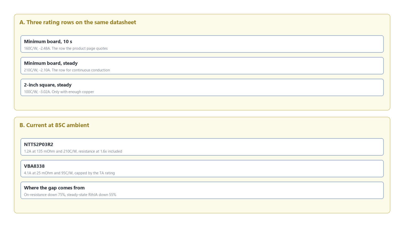
Figure 1. Three rating rows on NTTS2P03R2 and the current available at 85C ambient. The same minimum board gives -2.48A on a ten-second basis and -2.10A at steady state; at 210C/W and 135 mOhm, an 85C enclosure leaves 1.2A.
FAQ
Is NTTS2P03R2 obsolete? Yes. The lead-free version NTTS2P03R2G uses the same die and is obsolete as well; the difference is lead finish only.
Is the -2.48A rating a steady-state figure? No. It applies to a minimum FR-4 board at t <= 10 s. The same board at steady state is rated -2.10A, and the two rows differ by 50C/W.
How much current can it carry in an 85C enclosure? At 210C/W and 135 mOhm, 1.5A already reaches a 150C junction. Including the rise of resistance to about 1.6 times its 25C value, the practical figure is roughly 1.2A. Anything above 1.5A needs a different part or more copper.
How much does VBA8338 carry? -6.0A at 25C ambient. At 85C, 95C/W and 25 mOhm allow 5.2A thermally, but the TA rating near 85C is about 4.1A, so the lower of the two applies.
Is a -30V part enough on a 24V bus? 24V plus 20 percent is 28.8V, and plug-in ringing can pass 30V, which leaves thin margin. VBA8338 is also -30V, so that section does not change with substitution; more margin requires a higher voltage class.
Does Ciss rising from 500pF to 1600pF matter? The two figures are taken at different drain voltages, -24V and -15V, so they cannot be divided. On gate drive loss the difference is under a microwatt at 4.5V and 100 kHz.
What does a -3.0V threshold mean? The -1.0V to -3.0V span is a lot range, so the worst case needs 3.0V before conduction starts. With 3.3V drive only 0.3V of overdrive remains, a point outside the datasheet data.

Download PDF document
 Download now


