 中文
 English

Scenario Product Guide
Energy Storage Inverter Power Chain MOSFET Selection: VBL16R25SFD / VBGQA1802 /
 Back to previous page
Modern energy storage inverters are no longer simple battery-to-grid converters. As industrial parks, commercial buildings and microgrids move to battery energy storage systems (BESS), the inverter becomes a bidirectional power hub that must handle charging and discharging on the same hardware, at round-trip efficiencies consistently above 95%, inside an outdoor cabinet with limited airflow. Selecting MOSFETs for an energy storage inverter comes down to three decisions made at three different points in the power chain: the grid interface, the battery-side DC-DC stage, and the high-voltage DC link. This guide walks through each with the parameters that decide the outcome.
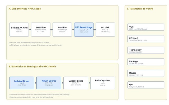
Figure 1. Grid interface / PFC stage of a bidirectional energy storage inverter — the rectified bus, the Super Junction boost switch and the DC link. The PFC switch is where body-diode reverse recovery sets the switching-loss floor.
1. Start with the voltage class at each stage
The most common specification error is applying one voltage class across the whole converter. An energy storage inverter has at least three distinct voltage domains, and each one has its own VDS requirement and its own safe margin.
| Power stage | Typical bus voltage | Required VDS class | Recommended margin |
|---|---|---|---|
| Battery-side DC-DC (low-voltage path) | 48–80 V | 80–100 V | 30–50% over max battery voltage |
| Battery-side DC-DC (400 V path) | 400 V | 600–650 V | 40–50% over bus |
| Grid interface / PFC | 400 VDC bus from 3-phase 400 VAC | 600–650 V | 40% over rectified peak |
| High-voltage DC link / auxiliary | 700–800 VDC | 1000 V | 20–25% over bus |
The margin is not conservatism for its own sake. During grid transients, battery over-voltage and load-dump events, the drain-source voltage can exceed the steady-state bus by 20% or more. A device rated exactly at the bus voltage will enter avalanche.
2. Match the technology to the stage, not to a single preference
Three MOSFET technologies cover the three stages of an energy storage inverter, and they are not interchangeable.
Commercially mature silicon for the low-voltage battery path. The battery-side DC-DC stage on a 48 V nominal rack operates at high current and low voltage. Shielded Gate Trench (SGT) MOSFETs are the correct choice here because the figure of merit (FOM = RDS(on) x Qg) is what governs loss in this synchronous buck-boost operating mode, and SGT delivers the lowest FOM in the 40–100 V range. A device such as VBGQA1802 (80 V / 180 A, 1.9 mΩ at VGS = 10 V, SGT, DFN8(5X6)) lets you build a high-current synchronous rectifier with a small footprint, which matters when the DC-DC board shares an enclosure with the battery management system.
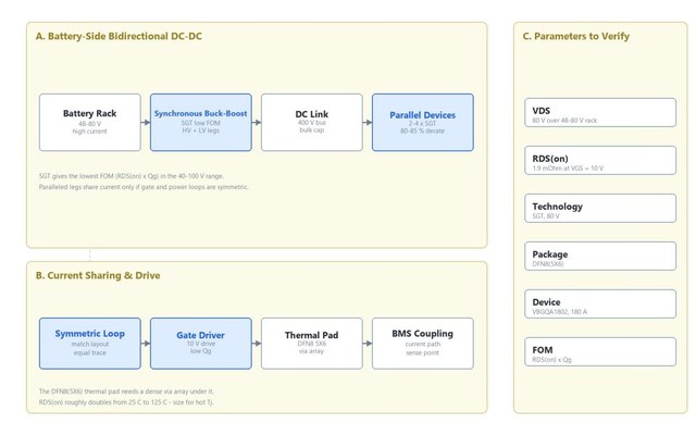
Figure 2. Battery-side bidirectional DC-DC stage. The SGT low-side and high-side legs carry the full rack current, so on-resistance measured at hot junction temperature and current sharing between paralleled devices decide the efficiency of this block.
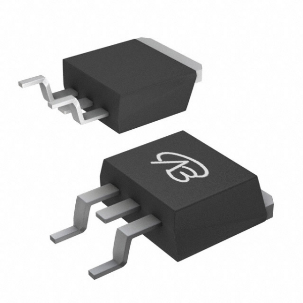
Super Junction silicon for the grid interface. The power factor correction and grid-tie stage runs from a rectified 3-phase 400 VAC input, giving a bus above 560 V. High-Voltage Silicon Super Junction MOSFETs are the established solution: the SJ_Multi-EPI structure achieves a low RDS(on) at a 600–650 V rating while keeping the output capacitance and gate charge low enough for 100–150 kHz operation, which shrinks the boost inductor. VBL16R25SFD (600 V / 25 A, 110 mΩ at VGS = 10 V, SJ_Multi-EPI, TO263) is representative of this class.
High-voltage silicon for the DC link and auxiliary rails. Where the DC link reaches 700–800 V — as it does in 3-phase 400 VAC systems and in 1500 V solar-coupled storage — a 1000 V class device is required. VBP110MR12 (1000 V / 12 A, 880 mΩ at VGS = 10 V, TO247) covers auxiliary power supplies, pre-charge circuits and high-voltage disconnect paths where the voltage headroom matters more than absolute conduction loss.
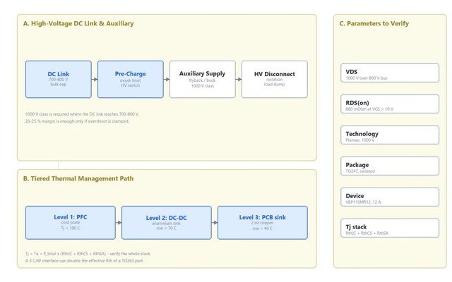
Figure 3. High-voltage DC link plus the tiered thermal path. The 1000 V class device covers pre-charge, auxiliary supply and disconnect functions; the lower panel shows how loss is spread across a cold plate, a heatsink and the PCB copper.
Note what is not on this list: you do not need SiC across the whole converter. Silicon Carbide (SiC) MOSFETs earn their premium in hard-switched bridges running above roughly 30 kHz, or where the body-diode reverse-recovery charge (Qrr) of silicon dominates loss. In a 20 kHz totem-pole PFC stage, the Qrr of a silicon MOSFET can dominate switching losses, and a 650 V SiC MOSFET cuts Qrr to near zero, reducing switching loss by roughly 40% at the same RDS(on). Below that frequency, or in soft-switched topologies, a Super Junction silicon device is the more cost-effective answer.
3. Recommended Power MOSFETs at a Glance
| Device | Type | VDS | Continuous Current | RDS(on) | Package | Role in This Solution |
|---|---|---|---|---|---|---|
| VBL16R25SFD | N-MOS (SJ_Multi-EPI) | 600 V | 25 A | 110 mΩ @10 V | TO263 | Grid interface / PFC and grid-tie stage main switch |
| VBGQA1802 | N-MOS (SGT) | 80 V | 180 A | 1.9 mΩ @10 V | DFN8(5X6) | Battery-side bidirectional DC-DC and synchronous rectification |
| VBP110MR12 | N-MOS (Plannar) | 1000 V | 12 A | 880 mΩ @10 V | TO247 | High-voltage DC link, auxiliary supply and pre-charge |
4. Balance conduction loss against switching loss
The single most expensive mistake in energy storage inverter design is selecting the MOSFET with the lowest RDS(on). Conduction loss and switching loss pull in opposite directions, and the minimum total loss is rarely at the minimum RDS(on).
Conduction loss in a MOSFET is P_cond = I²RMS x RDS(on) x D, where D is the duty cycle. Switching loss is approximately P_sw = (Eon + Eoff) x fsw, plus output-capacitance loss P_Coss = 0.5 x Coss x V² x fsw. The two move against each other: a die with a lower RDS(on) carries more silicon area, which raises Coss and Qg, which raises switching loss. At 100 kHz and above, the switching term can overtake the conduction term entirely.
Two consequences follow for a BESS converter:
- RDS(on) must be evaluated at operating junction temperature, not at 25 °C. Silicon MOSFET on-resistance roughly doubles between 25 °C and 125 °C. A part specified at 1.9 mΩ on the datasheet contributes about 3.4–4 mΩ of real resistance in a cabinet running at 80 °C ambient with a 110 °C junction. Any loss calculation done at 25 °C will understate conduction loss by nearly half.
- Coss, not just RDS(on), must be checked in a high-frequency stage. The energy stored in the output capacitance (Eoss) is dissipated every switching cycle in a hard-switched topology. For a 600 V device switching at 100 kHz, Eoss in the tens of microjoules per cycle becomes several watts of loss per device.
5. Verify thermal path and packaging before committing
Datasheet ratings describe the die, not the assembly. Three checks close the gap:
- Calculate junction temperature end to end. Tj = Ta + P_total x (RthJC + RthCS + RthSA). A 3 °C/W cold-plate interface can double the effective thermal resistance of a TO263 part, so a device that looks comfortable at 2.5 °C/W RthJC may exceed its limit in the real cabinet.
- Choose the package for the thermal path you actually have. TO247 provides a large, isolated mounting surface for a cold plate or a forced-air heatsink and is appropriate for the high-voltage DC link. TO263 conducts heat through the PCB copper and is well matched to a surface-cooled DC-DC board. DFN8(5X6) parts rely on an exposed thermal pad and a dense thermal via array, so the PCB copper area under the pad is a design parameter, not a layout afterthought.
- Account for paralleling. Paralleled SGT MOSFETs sharing a DC bus will not share current equally unless the gate loop and the power loop are symmetric. Use a Kelvin source connection where the package provides one, and derate the pair to 80–85% of the sum of their ratings.
Selection checklist
- List every voltage domain in the converter and assign a VDS class with a 20–50% margin.
- Decide per stage whether the design is hard-switched above 30 kHz; only then consider SiC.
- Compute P_cond at maximum ambient junction temperature, using the hot RDS(on) estimate.
- Compute P_sw including Eoss, and compare the sum against the alternative candidate.
- Select the package from the available thermal path, then verify Tj with the full resistance stack.
- Confirm the gate drive can deliver the required Qg at the target fsw without exceeding driver loss budget.
Need application-specific data, thermal calculations or samples for your BESS converter design? Contact our engineering team for the full parametric datasheets of VBL16R25SFD, VBGQA1802 and VBP110MR12.
Frequently Asked Questions
Q: Which device is recommended for the grid interface / PFC stage of an energy storage inverter?
A: VBL16R25SFD (600 V / 25 A / TO263, SJ_Multi-EPI). A 600 V rating holds a 40% margin over the rectified peak of a 3-phase 400 VAC input, and the 110 mΩ on-resistance at VGS = 10 V keeps conduction loss low in the boost stage at 100–150 kHz.
Q: Which device is recommended for the battery-side DC-DC stage?
A: VBGQA1802 (80 V / 180 A / DFN8(5X6), SGT). Its 1.9 mΩ on-resistance at VGS = 10 V and 180 A continuous rating let you build a high-current synchronous buck-boost or rectifier on a small board, and SGT gives the lowest figure of merit in the 40–100 V range.
Q: Which device covers the high-voltage DC link and auxiliary supplies?
A: VBP110MR12 (1000 V / 12 A / TO247, Plannar). A 1000 V class is required where the DC link reaches 700–800 V, covering pre-charge circuits, auxiliary power supplies and high-voltage disconnect paths.
Q: Do I need SiC MOSFETs in an energy storage inverter?
A: Not across the whole converter. Silicon Carbide pays off in hard-switched bridges above roughly 30 kHz, or where the silicon body-diode reverse-recovery charge (Qrr) dominates loss. Below that frequency, or in soft-switched and clamped topologies, a Silicon Super Junction device is the more cost-effective choice.
Q: Why does MOSFET on-resistance have to be evaluated at hot junction temperature?
A: Silicon on-resistance roughly doubles between 25 °C and 125 °C. A loss calculation using the 25 °C datasheet value understates conduction loss by nearly half, which is why cabinets meet their efficiency target when cold and miss it under sustained load.

Download PDF document
 Download now:VBL16R25SFD


Request Free Samples
*To request free samples, please complete and submit the following information.
Our team will review your application within 24 hours and arrange shipment upon approval. Thank you!