 中文
 English

Scenario Product Guide
Portable Power Station MOSFET Selection: VBL7603 / VBL16R41SFD / VBL2625
 Back to previous page
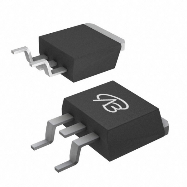
A portable power station packs a battery pack, a bidirectional converter and a pure-sine inverter into one enclosure, and every watt that reaches the AC outlet has already passed through at least two MOSFET stages. Unlike a rack-mounted energy storage system, the portable unit runs at a 48 V battery bus, sits on a floor next to a user, and has no active cooling beyond a small fan. Those three constraints - low bus voltage, high current, and almost no thermal headroom - decide the entire device selection. This guide walks the power chain stage by stage and maps each stage to a device class, with one worked example per stage.
At a glance
Three stages decide efficiency: battery-side synchronous buck-boost, AC output inverter, and high-side protection switching.
Voltage class follows the bus, not the nameplate: a 48 V pack needs 60 V devices, a 220 VAC output needs 600 V devices.
Conduction loss dominates below 60 V and switching loss dominates above 400 V - the two ends of the chain need opposite optimizations.
Recommended device comparison
| Device | Type | VDS | ID | RDS(on) @10V | Package | Role in this design |
|---|---|---|---|---|---|---|
| VBL7603 | Dual-N+N | 60V | 150A | 2 mΩ | TO263-7L | Battery-side synchronous buck-boost, both switches in one package |
| VBL16R41SFD | Single-N | 600V | 41A | 62 mΩ | TO263 | AC output inverter leg, SJ_Multi-EPI |
| VBL2625 | Single-P | -60V | -80A | 19 mΩ | TO263 | High-side load switch and reverse-battery protection |
| VBM1101N | Single-N | 100V | 100A | 9 mΩ | TO220 | DC output and USB-PD pre-regulation stage |
One. Why the 48 V bus fixes the voltage class
(a) The battery side is a 60 V design, not a 48 V design
A 13S lithium-ion pack swings between roughly 39 V empty and 54.6 V full, and a 48 V nominal bus is the industry shorthand for that range. Selecting a 48 V rated device leaves 12 percent headroom at full charge, which is not enough once hot-plug transients and cable inductance spikes are added. The practical rule is to size the device for at least 1.25 times the maximum pack voltage, which lands on the 60 V class.
VBL7603 sits exactly there: 60 V, 150 A continuous, 2 mΩ at 10 V gate drive, in a TO263-7L package. What matters more than any single number is its configuration - Dual-N+N, meaning two N-channel MOSFETs in one package with a common node already bonded. A synchronous buck-boost half bridge is exactly two N-channel devices with a shared switching node, so one package replaces two discrete parts, halves the loop inductance between them, and removes one gate loop from the layout.
(b) The AC side is a 600 V design
A 220 VAC sine wave peaks at 311 V. A 600 V device therefore carries a 93 percent margin against the nominal peak, and still survives the inductive kick that a motor load or a reactive appliance reflects back into the inverter leg. Going to 650 V or 700 V buys nothing here and costs RDS(on): at the same die size, every extra 100 V of rating roughly doubles the on-resistance, and on-resistance is what you pay for continuously.
VBL16R41SFD is a 600 V, 41 A single N-channel device with 62 mΩ on-resistance in TO263, built on SJ_Multi-EPI super junction technology. The super junction structure is what makes 62 mΩ possible at 600 V - a planar device at the same rating would sit an order of magnitude higher, as the 700 V, 4 A, 3200 mΩ planar part in the same family shows.
Two. Stage-by-stage selection
(a) Battery-side synchronous buck-boost
This stage has to work in both directions: boost when the pack feeds the inverter, buck when a wall charger refills the pack. A four-switch buck-boost uses two half bridges, and each half bridge is one VBL7603 package. With 2 mΩ on-resistance, the conduction loss at 100 A is 20 W in the switch that is fully on; the same current through a 19 mΩ device would be 190 W, which no passive heatsink in a portable enclosure can remove.
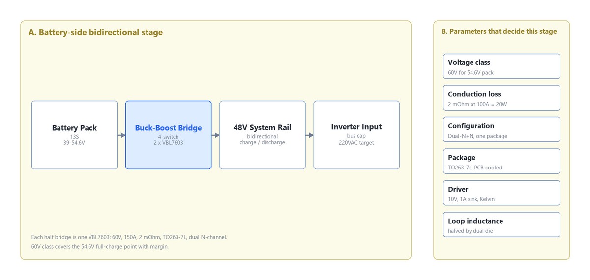
Figure 1. Battery-side bidirectional stage: the pack connects through a four-switch buck-boost, one VBL7603 per half bridge, before reaching the 48 V system rail.
(b) AC output inverter leg
The inverter leg carries the full load current at a switching frequency between 16 kHz and 40 kHz, high enough to keep the output filter small and low enough to stay inside the EMI budget of a consumer product. Two things follow. First, 41 A of continuous rating leaves room for the 2 kW surge that a compressor or a motorized tool demands for a few hundred milliseconds. Second, the body diode must recover cleanly, because a hard-switched leg at 600 V turns the low-side body diode on during every dead time; the Qrr of that diode is the switching loss you cannot design away with a bigger heatsink.
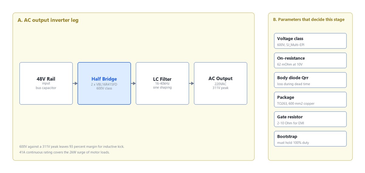
Figure 2. AC output inverter: two VBL16R41SFD per leg, 600 V class against a 311 V peak, followed by the LC output filter and the AC receptacle.
(c) High-side switching and reverse-battery protection
A P-channel device in the high side needs no charge pump: pull the gate to ground and the switch is on, tie it to the source and the switch is off. In a product that ships to end users and gets connected to whatever charger is at hand, that simplicity is worth more than the on-resistance penalty. VBL2625 is a -60 V, -80 A P-channel device with 19 mΩ at 10 V drive in TO263. Two of them back to back in the battery return path give reverse-polarity blocking without a fuse in the main current path.
Where the load is a regulated DC output rather than the AC inverter, VBM1101N covers the 100 V, 100 A, 9 mΩ corner in TO220 and suits a pre-regulation stage feeding a USB-PD controller.
Three. System-level checks that decide whether the BOM works
(a) Gate drive differs at the two ends of the chain
The 60 V devices want 10 V of gate drive to reach their rated on-resistance, and their gate charge is large enough that a weak driver turns the switching loss into heat. Drive VBL7603 from a dedicated gate driver with at least 1 A peak sink current, keep the gate loop under 10 mm, and use a Kelvin source connection. The 600 V inverter devices need a different treatment: 10 to 12 V drive, a 2 to 10 Ω series gate resistor to slow the dv/dt into the EMI budget, and a bootstrap supply that holds up during the 100 percent duty excursion some inverters use at peak output.
(b) Thermal path, not thermal mass
A portable enclosure has no room for a large heatsink, so the TO263 packages must dump heat into copper. Give each device at least 600 mm2 of copper on the drain tab, stitch that copper to the inner layers with a via array, and treat the PCB itself as the heatsink. The TO263-7L package of VBL7603 helps here because the extra pins carry current rather than heat, leaving the tab free for thermal transfer.
(c) What to verify before the first prototype
Measure the switching node overshoot at full load with the real cable length attached - a portable unit is used with whatever cord the customer owns.
Check the inverter leg temperature at 40 degrees ambient, not at 25 - the enclosure traps air.
Confirm the reverse-protection pair does not conduct through its body diode when the pack is inserted backwards, then confirm it does conduct forward.
Four. What this selection buys
Two device classes cover the whole chain: 60 V for everything that touches the battery, 600 V for everything that touches the grid-side output. Within each class, the choice is driven by package and configuration rather than by headline current - the dual N-channel package halves the loop inductance at the battery side, and the super junction process is what makes a 62 mΩ, 600 V, 41 A device fit in a TO263 on the AC side. The result is a power chain that a small fan can cool, which is the actual constraint in a portable product.
FAQ
Q: Which device drives the battery-side converter in a 48 V portable power station?
A: VBL7603, a 60 V, 150 A dual N-channel device at 2 mΩ in TO263-7L. The 60 V rating covers the 54.6 V full-charge point of a 13S pack with margin, and the dual configuration puts both switches of a half bridge in one package.
Q: Why 600 V for a 220 VAC output instead of 650 V?
A: 220 VAC peaks at 311 V, so 600 V already provides a 93 percent margin. Raising the rating to 650 V increases on-resistance at the same die size, and that on-resistance is paid continuously in conduction loss.
Q: Can a P-channel device handle the main battery current?
A: Yes when the current path allows 19 mΩ. VBL2625 is rated -60 V and -80 A at 19 mΩ in TO263, and it removes the charge pump that an equivalent N-channel high-side switch would require.

Download PDF document
 Download now:VBL7603


Request Free Samples
*To request free samples, please complete and submit the following information.
Our team will review your application within 24 hours and arrange shipment upon approval. Thank you!