 中文
 English

Scenario Product Guide
MOSFET Selection in 140W USB-C PD Chargers: Loss Trade-offs
 Back to previous page

A 140W USB-C PD charger (28 V at 5 A, PD 3.1 EPR) has four switch positions: the PFC switch, the LLC primary half-bridge, the secondary synchronous rectifiers, and the VBUS disconnect. At this power level the conduction loss in every one of those positions stays under 0.2 W, so the choice is decided by switching loss, gate drive and package rather than by RDS(on). This applies to 90–264 Vac input designs that use a boost PFC followed by an LLC or an active-clamp forward. Above roughly 250 W the balance flips back: conduction loss grows with the square of the current, and a 56–75 mΩ silicon device becomes cheaper than a 110 mΩ GaN part.
At a glance
- Switching loss, not on-resistance, decides the PFC and primary positions at 140W — a 110 mΩ e-mode GaN device can beat a 75 mΩ super junction MOSFET in continuous-conduction PFC.
- The 28 V output fixes secondary rectification in the 100V class; 150V parts cost 1.5–2× the RDS(on) at the same die area and buy margin the topology does not need.
- The VBUS disconnect and port protection belong to the 40V class, where a 0.7 mΩ LFPAK56 device replaces a much larger 100V die.
Why a 140W charger is not a scaled-down 65W charger
A 65W adapter can be a single flyback: one primary switch, one secondary diode or synchronous rectifier, and no power-factor correction, because EN 61000-3-2 Class D only applies above 75 W. Crossing 75 W forces a second conversion stage, and that stage has the opposite optimisation target from the first. The PFC runs in continuous conduction at a 400 V bus with hard switching, so its device pays reverse-recovery and output-capacitance loss on every cycle. The LLC runs with zero-voltage switching, so its device pays almost no turn-on loss but must survive the resonant ring. The rectifiers are timed by the transformer, not by a controller, so their body diode conducts during every commutation gap.
Four positions, four different loss mechanisms, one BOM. That is why picking a single "best" MOSFET family for the whole charger produces a design that is either expensive or hot, and usually both.
The four switch positions and what decides each
| Design variable | Range in a 140W charger | What it decides | Device class |
|---|---|---|---|
| Input voltage | 90–264 Vac | PFC switch voltage margin | 650V |
| PFC conduction mode | CCM above 100 kHz, or BCM | Reverse-recovery tolerance | GaN (no Qrr) vs super junction |
| DC bus | 380–410 V | LLC primary rating | 650V |
| Output | 5–28 V, 5 A | Rectifier rating | 100V |
| Port protection | 28 V plus hot-plug ring | Disconnect switch rating | 40V |
| Switching frequency | 100–300 kHz for the LLC | Gate charge budget | DFN8 / LFPAK56 |
The table is deliberately ordered by consequence, not by voltage. The input range and the conduction mode together remove more candidate parts than every other row combined, because a super junction device in CCM PFC at 300 kHz is thermally impossible while the same device in BCM is entirely fine.
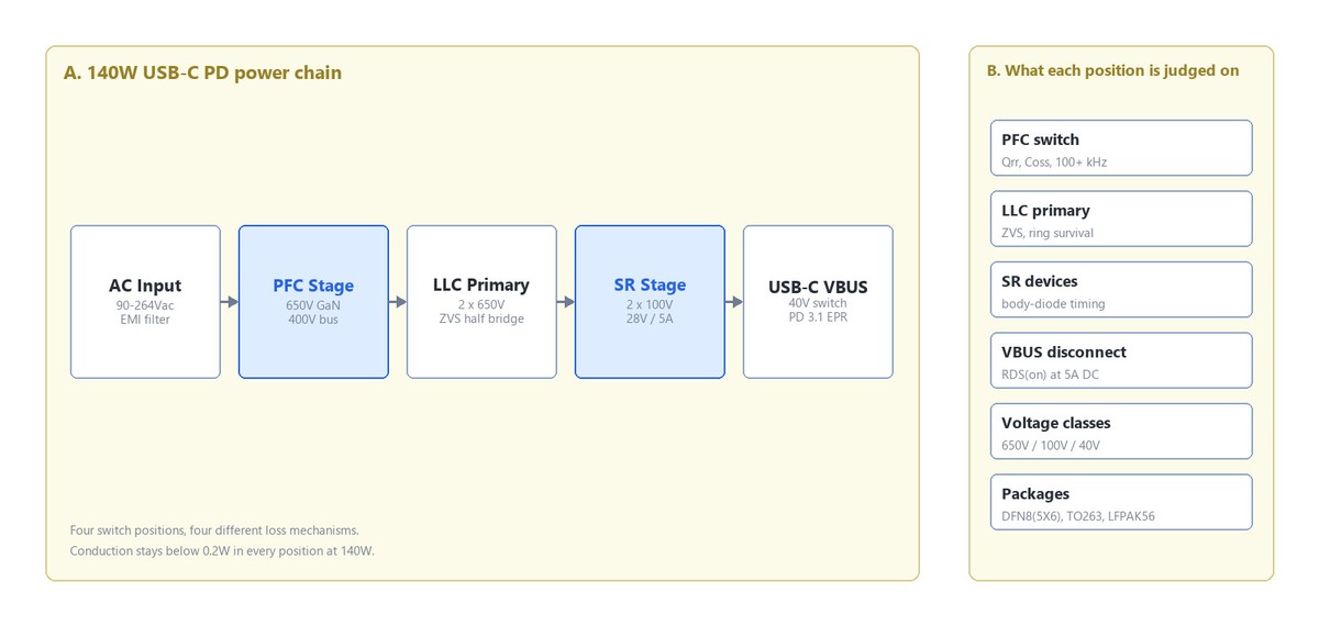
Figure 1. Four switch positions in a 140W USB-C PD charger: PFC at 650V, LLC primary at 650V, synchronous rectification at 100V and a 40V VBUS disconnect.
Recommended device comparison
Four positions, four parts. Every rating below is taken from the published datasheet for that part number.
| Model | Type | VDS | ID | RDS(on) | Package | Position in this design |
|---|---|---|---|---|---|---|
| VBQA165A20S | GaN e-mode HEMT | 650V | 20A | 110 mΩ at 6 V | DFN8(5X6) | PFC switch and LLC primary, hard-switched |
| VBL165R36S | Super junction | 650V | 36A | 75 mΩ at 10 V | TO263 | LLC primary half-bridge where cost dominates |
| VBGED1103 | SGT N-channel | 100V | 180A | 3.0 mΩ at 10 V | LFPAK56 | Secondary synchronous rectification, both legs |
| VBGED1401 | SGT N-channel | 40V | 250A | 0.7 mΩ at 10 V | LFPAK56 | VBUS disconnect and port protection |
The 650V class in VBsemi's published selector lists 194 part numbers, the 100V class 123 and the 40V class 57. The corner this design needs — 650V in DFN8(5X6), 100V and 40V in LFPAK56 — exists in all three, which is what makes a single-vendor BOM possible without accepting a package compromise at any one position.
Engineering trade-offs: conduction, switching and gate drive
Conduction is not the deciding loss at 140W. At 115 Vac input the PFC carries about 1.22 A RMS. In a 110 mΩ device that is 0.16 W; in the 75 mΩ VBL165R36S it is 0.11 W. The difference, 50 mW, is smaller than the tolerance on a single gate-drive resistor. Anyone choosing silicon over GaN because 75 is less than 110 is optimising the wrong term.
Reverse recovery is the deciding loss. A super junction MOSFET at 650 V has a body diode, and in CCM PFC that diode is forced to recover on every switching cycle. The loss is the product of recovery charge, bus voltage and frequency: 200 nC of Qrr at a 400 V bus and 100 kHz is already 8 W, which is more than 5% of a 140W output. No heatsink inside a 65 × 65 mm adapter can remove 8 W quietly. The choice therefore is not "GaN or silicon" but "GaN at 100 kHz CCM, or silicon at 65 kHz boundary conduction with a physically larger inductor". Both are valid products; they are not interchangeable.
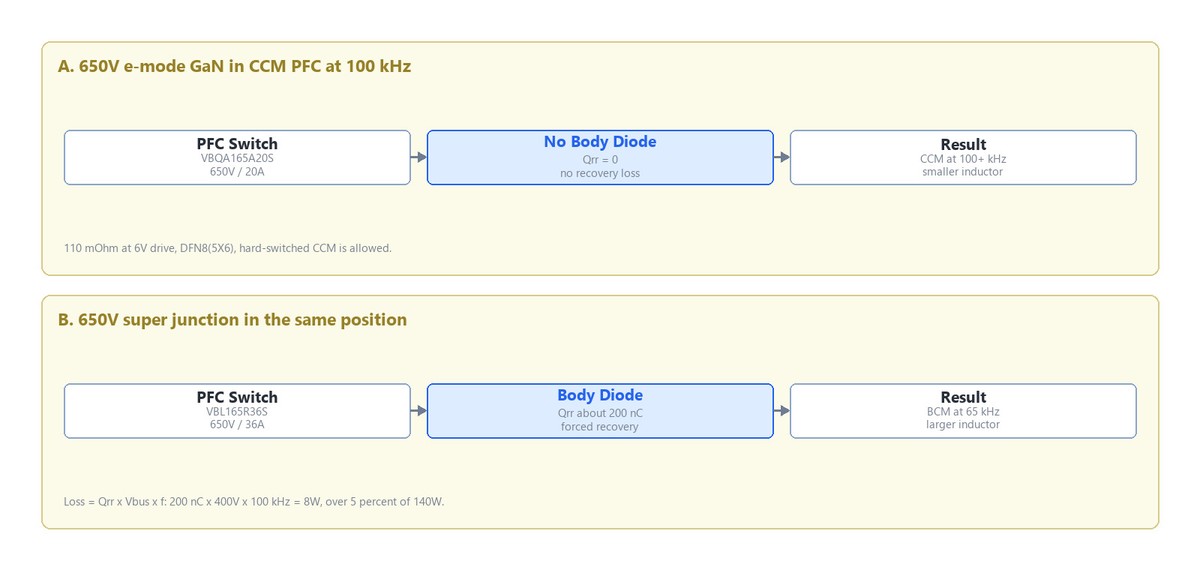
Figure 2. The same PFC position with e-mode GaN and with super junction silicon: zero recovery charge allows continuous conduction at 100 kHz, while 200 nC of Qrr at 400 V and 100 kHz already costs 8 W.
Gate drive is where the cost hides. An e-mode GaN device such as the VBQA165A20S wants 6 V on the gate with a 7 V absolute maximum and a −1.5 V floor, so the driver must be a regulated 0–6 V type with a tight clamp, and the layout must keep the gate loop under a few millimetres. A super junction device is happy with 10 V and tolerates the sloppier drive that a low-cost controller provides. The GaN saves the inductor and the heatsink but adds a dedicated driver.
The rectifiers are a timing problem, not a resistance problem. At 28 V output, a 100V device carries 5 A DC with a 3.5× margin. What matters is that the body diode conducts only briefly and that the gate is pulled off before the primary starts the next cycle; the 3.0 mΩ channel of the VBGED1103 makes that window comfortable rather than critical.
Package, not die, decides the thermal path. In an adapter with no fan the LFPAK56 source pad is the heatsink. The 0.7 mΩ VBGED1401 at 40 V dissipates 17 mW at 5 A, so its thermal design is driven by the PCB copper it sits on rather than by the device itself. The DFN8(5X6) GaN part is the opposite case: the die is small, and the switching loss it generates has to leave through a 5 × 6 mm pad.
Four mistakes that cost efficiency or yield
- Up-rating the rectifiers "for margin". Moving from 100V to 150V at the same package roughly doubles RDS(on). At 28 V output the transformer clamp bounds the ring, so the extra 50 V buys nothing and costs conduction loss at 5 A continuously.
- Driving e-mode GaN with a 10 V silicon driver. The gate oxide of an e-mode HEMT is not a MOSFET gate oxide. 10 V exceeds the 7 V maximum, and the failure is immediate and silent until the first thermal cycle.
- Switching to GaN without redesigning the PFC inductor. The point of GaN is the higher frequency. Keeping the original inductor means paying the GaN price and keeping the silicon-size magnetics, which is the most common way a GaN upgrade produces no measurable efficiency gain.
- Using a 100V device for the VBUS disconnect. The disconnect carries 5 A DC and blocks 28 V. A 40V, 0.7 mΩ part in LFPAK56 does the job with a quarter of the die area and a fraction of the gate charge.
Where this selection stops working
Above about 250 W the RMS currents in the PFC and the primary double, conduction loss quadruples, and the 110 mΩ GaN device starts to need parallel parts — at that point 56–75 mΩ silicon in TO247 becomes the cheaper answer. Below 65 W the second stage disappears entirely and a single flyback with an integrated switch beats any discrete plan. And if the design must survive a 2 kV surge without an external clamp, an e-mode GaN device is the wrong choice, because it has no avalanche rating to absorb the energy; a super junction device with a specified avalanche capability belongs there instead.
FAQ
Q: Can a 650V e-mode GaN device replace a 650V super junction MOSFET pin for pin?
A: No. The gate drive window is 0–6 V with a 7 V maximum instead of ±20 V, the source-sense pin is separate, and the package footprint differs. It is a board redesign, not a drop-in, and the driver IC usually changes with it.
Q: Why 100V for the secondary rectifier when the output is only 28 V?
A: Because the rectifier blocks the reflected primary voltage plus the leakage-inductance ring, not the output voltage. 28 V output with a 3.5× ring lands near 100 V, and a 100V part at 3.0 mΩ is smaller and faster than a 150V part at the same current.
Q: Is 110 mΩ too high for a 140W PFC switch?
A: No. At 115 Vac the PFC carries about 1.22 A RMS, so 110 mΩ dissipates 0.16 W. The switching loss in the same device dominates by an order of magnitude, and on-resistance only becomes the limiting term above roughly 250 W.
Q: What decides between DFN8(5X6) and TO263 for the 650V parts?
A: Thermal path and assembly. DFN8(5X6) is the smaller footprint and suits a GaN die with low conduction loss; TO263 gives a larger drain tab for PCB cooling and is the practical choice when a 75 mΩ silicon die has to shed more heat.
Q: How should the four positions be split between GaN and silicon?
A: Use GaN where the device is hard-switched at high frequency — the PFC — and silicon where the switching loss is already removed by the topology, such as a zero-voltage-switched LLC. Mixing the two technologies in one charger is normal, and VBsemi supplies both classes in the same surface-mount packages so the two halves of the BOM do not fight over footprints.

Download PDF document
 Download now:VBQA165A20S


Request Free Samples
*To request free samples, please complete and submit the following information.
Our team will review your application within 24 hours and arrange shipment upon approval. Thank you!