 中文
 English

IRF7504TRPBF Dual P-Channel MOSFET Power Selection: 12V Gate Limit
 Back to previous page

IRF7504TRPBF is the orderable code for the IRF7504: -20V, dual P-channel, Micro8 eight-pad, 4000 per reel, lead-free. Its most common home is not a switching converter — it is the first stage at the power inlet, the part that blocks current when a battery is inserted backwards, or keeps an adapter and a battery on one rail without either feeding the other. Two things define that position, and both have to be settled before any substitution study: the device conducts 100% of the time rather than switching, and at the instant of a reversed insertion the full pack voltage lands across gate and source.
At a glance
It sits at the inlet: reverse-battery blocking, two-supply OR-ing, system disconnect. In normal operation it is a path, not a switch.
Gate-to-source voltage at that position equals the pack voltage: about −Vbat when wired right, +Vbat when reversed. Both directions run the gate at full battery amplitude.
The original's gate rating is only ±12V, which leaves zero margin. A 24V rail (two lead-acid blocks, six lithium cells) cannot use it directly.
VBA9338 is rated ±20V, so the clamp network can go, and on-resistance drops from 270mΩ to 55mΩ at 4.5V.
The only cost is gate charge, 8.2nC to 25nC — and at a position that switches a few thousand times a year, that cost does not apply. The opposite conclusion holds in load-switch duty.
Where the part actually sits
The positions share one property: once on, they stay on, with no high-frequency content in between.
| Position | How it is wired | What the position demands |
|---|---|---|
| Reverse-battery blocking | One P in series with the positive terminal, source toward the load, gate to the battery negative | Gate must survive the whole pack voltage; on-resistance sets the drop |
| Two-supply OR-ing | One device per source, gates cross-coupled to the opposite rail | Matched pair; gate swing equals the difference between the two rails |
| System disconnect | One device between battery and load, gate pulled low by a key or an MCU | Low leakage when off; the drop must not eat the downstream minimum input |
None of these regulate, and none switch at frequency. They are paths: on or off. Whether a part survives here depends on what it can hold off and how much voltage it drops while conducting — not on how fast it can switch.
Why P-channel, and why often dual
There is exactly one reason to use P here: the source ties to the positive rail, and pulling the gate to ground turns it on. No bootstrap capacitor, no charge pump. An N-channel doing entry-level reverse protection needs a gate drive above the bus, and on a small board that arithmetic rarely works out.
Dual exists because the inlet often needs two paths: one device blocks reverse insertion, the other disconnects the system; or one per source in an OR-ing pair. A Micro8 holds two independent dice with D1 and D2 brought out separately (pins 7-8 and 5-6), and the package is under 1.1mm thick — which is why it ended up in portable gear.
For a substitution, "dual" means two things: both dice get checked separately, and the pinout has to match one-for-one. Eight-pad dual P-channel parts come in common-drain and isolated configurations; the package looks identical and the internal wiring does not.
At the instant of reversal, the gate sees the whole pack
Take the common wiring: battery positive to drain, load to source, gate through a resistor to the battery negative.
Wired correctly, the body diode first lifts the source to Vbat minus a forward drop, the gate sits at 0V, so VGS is about −(Vbat − Vf) and the channel turns on hard, shorting out the diode.
Insert the battery backwards and that gate line — which was tied to the negative terminal — now sits on the positive terminal, while the source side is near 0V. VGS becomes about +Vbat and the device blocks. That is exactly the event it is there to block.
Both directions see the absolute value of the pack voltage. The original's absolute maximum gate rating is ±12V, and that single number decides which rail it can live on:
| Rail | Original, ±12V | VBA9338, ±20V |
|---|---|---|
| Single lithium cell, 3.0–4.2V | comfortable | comfortable |
| 12V (three cells at 12.6V, or lead-acid) | sits on the limit, transients exceed it | 8V left over |
| 24V (six cells at 25.2V) | zener clamp mandatory | usable as-is |
"Sits on the limit" is not a figure of speech. An absolute maximum of 12V means the gate oxide may be damaged above it, and a fully charged 12.6V pack with no current limiting at the reversal instant has nothing to absorb the overshoot. On a 12V rail, the clamp on the original is not optional.
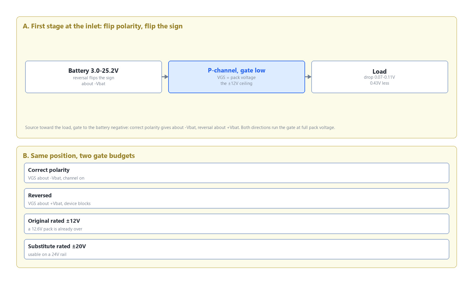
Figure 1. At the inlet the gate sees the whole pack voltage: about -Vbat when the battery is in correctly, +Vbat when it is reversed. A ±12V part has zero margin on a 12V rail.
What changes with VBA9338
Same package, same dual P-channel arrangement; the differences are voltage class, conduction and charge:
| Parameter | IRF7504TRPBF | VBA9338 | Change |
|---|---|---|---|
| VDS | -20V | -30V | 10V more |
| Gate rating | ±12V | ±20V | 8V more |
| RDS(on) @4.5V | 270mΩ | 55mΩ | 1/4.9 |
| RDS(on) @10V | not given | 38mΩ | — |
| Qg | 8.2nC max | 25nC typ | 3x higher |
| RthJA steady state | 100 K/W | 85 K/W | 15% better |
At this position the first three rows are all gain, and the gain most often underestimated is not resistance — it is forward drop:
| Load current | Original drop | Substitute drop |
|---|---|---|
| 0.5A | 0.135V | 0.028V |
| 1.2A | 0.324V | 0.066V |
| 2A | 0.540V | 0.110V |
In a 3.7V lithium system, 0.54V is 14.6% of the pack voltage. If the downstream stage is an LDO with a 3.0V minimum input, then at a 3.5V pack the original leaves 2.96V — not enough — while the substitute still has 3.39V. What that gap buys is not an efficiency percentage; it is whether the last stretch of battery capacity is usable at all.
The fourth row is the cost, and here it does not apply. Reverse blocking and system disconnect switch a few thousand times a year; gate charge is spent only at the edges, and the difference between 25nC and 8.2nC spread over a few thousand events is negligible. The same substitute in a load-switch role is a different story — the IRF7504 note works through the crossover current. At the inlet, gate charge does not enter the decision.
The two positions, judged separately
Reverse-battery blocking — swap directly, but review the gate network first. With a ±20V part, the zener clamp that existed for ±12V can come out, provided you first establish the highest voltage on the whole rail: charger open-circuit voltage, hot-plug transient, and the reversal event itself. Removing a clamp saves two components and gives up the second line of defence.
Two-supply OR-ing — swap both. The two devices must be the same part from the same lot, or the two paths will drop different voltages and, at handover, current back-feeds from the lower-drop path into the higher one. Changing one device looks fine on paper and shows up only on the switching waveform.
Five things to check before the swap
Pinout and internal structure. Dual P in eight pads comes as common-drain or isolated. Compare pin assignment pad by pad before any prototype.
Highest gate-loop voltage. Not the nominal pack voltage — full charge plus transients.
Downstream minimum input. The drop is smaller now; the under-voltage trip and low-battery warning thresholds may need to move with it.
Matching of the two dice. Check both channels separately; do not extrapolate from one channel's typical value.
Packaging and moisture. The original is 4000 per reel, lead-free, MSL 1. Re-check feeder setup and any bake step against the new part's declaration.
Three cases where you should not swap
The rail is low and the drop does not hurt. On a 3.3V or 5V inlet at modest current, nobody notices 0.1V, and the swap buys only a qualification cycle.
There is reverse surge or hot-plug on the board, and the 12V gate was verified as just enough. Here the swap improves margin rather than addressing the original failure mechanism — find out why the first design was marginal before changing parts.
Customer drawings or the approved vendor list name the original. Drawing revision plus customer sign-off and AVL re-qualification all run on prototype time. The shared eight-pad package will not change; the paperwork will.
For the same part spread across four positions, the IRF7506TRPBF note breaks it down position by position, including how the thermal budget sets the real current limit.
FAQ
Are IRF7504 and IRF7504TRPBF the same part?
Same die. TR is tape and reel, PBF is lead-free, and only IRF7504TRPBF is orderable. Both codes are marked obsolete; what circulates is inventory.
On a 12V battery, does a ±12V gate really get exceeded?
Yes. A fully charged 12.6V pack already exceeds the absolute maximum, and the reversal instant has no current limiting. On that rail the clamp stays.
Once the part is ±20V, can the zener simply be removed?
Establish the highest voltage on the rail first — charger open-circuit, hot-plug transient, reversal transient. If all of them stay under 20V, it can go, accepting that one layer of protection goes with it.
Does Qg rising from 8.2nC to 25nC matter for reverse blocking?
Barely. A few thousand switching events a year make the drive loss negligible. What does matter is that the edge stays fast enough; a slow edge keeps the device in its linear region longer at power-up.

Download PDF document
 Download now


