 中文
 English

Scenario Product Guide
VBsemi VBGQA1301 SGT MOSFET – The Precision Choice for AI Server Power Supply
 Back to previous page

Power Management Challenges in the Era of Explosive AI Computing Power
With the exponential growth in demand for generative artificial intelligence and large language model training, the power density and power supply complexity of AI server clusters are facing severe challenges. Efficient, compact, and reliable power solutions have become the underlying key to supporting the continuous expansion of computing power. Against this backdrop, VBsemi's VBGQA1301 SGT MOSFET, with its superior electrical performance and optimized packaging, precisely addresses the core requirements of AI server power supplies for high efficiency, high power density, and fast transient response.
In-depth Technical Analysis: How VBGQA1301 Achieves Performance Breakthrough
Core Technological Innovation: Integration of SGT Structure and Advanced Packaging
The VBGQA1301 employs shielded gate trench technology, significantly reducing switching losses and gate charge through optimized charge balance and electric field management. Its advanced DFN8 5X6 package provides excellent electrical performance while achieving a very small footprint and lower thermal resistance, making it particularly suitable for space-constrained, high-density server power supply designs. The device exhibits extremely low on-resistance at both 4.5V and 10V drive voltages, ensuring efficient switching from light load to full load.
Key Parameter Comparison Analysis: Comprehensive Performance Leading the Way
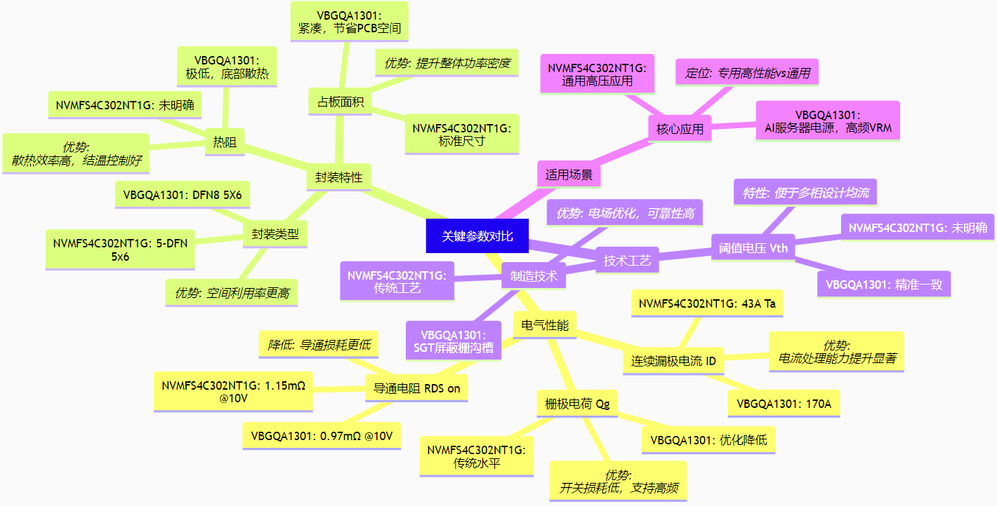
Figure 1: Comparison and analysis of key parameters between VBGQA1301 and NVMFS4C302NT1G
Compared to ON Semiconductor's comparable model, the NVMFS4C302NT1G, the VBGQA1301 outperforms it in several key metrics. Its continuous drain current reaches 170A, significantly exceeding the comparable model's 43A (Ta), demonstrating a substantial improvement in current handling capability and providing ample margin for handling the instantaneous high current demands of AI accelerator cards. Regarding the core on-resistance, the VBGQA1301 achieves only 0.97mΩ at 10V drive, superior to the comparable product's 1.15mΩ, resulting in lower conduction losses. Furthermore, its compact DFN8 5x6 package offers greater space utilization compared to the traditional 5-DFN (5x6) package, contributing to improved overall power density.
Core application scenarios in AI server power architecture
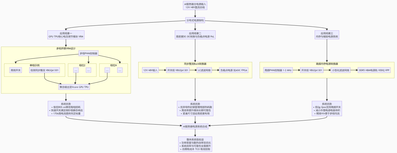
Figure 2: Core Application Topology of VBGQA1301 in AI Server Power Architecture
GPU/TPU Core Voltage Regulation Module
In multi-phase parallel VRM designs, the VBGQA1301's extremely low RDS(on) and high current capability effectively reduce power loss per phase and improve overall conversion efficiency. Its fast switching characteristics help meet the stringent requirements of modern GPUs/TPUs for microsecond-level transient load changes, ensuring stable power supply to the computing core.
High-Density DC-DC Conversion and Point-of-Load Power Supply
In 12V/48V point-of-load (PoL) distributed power architectures, this device is ideal for building efficient synchronous rectified buck converters. Its superior thermally conductive package design, combined with bottom heat dissipation, effectively manages localized heat dissipation, improving the long-term reliability of the module.
Memory and Auxiliary Power System
With the increasing power consumption of DDR5 and HBM memory, the power supply for them needs to be both highly efficient and compact. The VBGQA1301 supports high-frequency switching, which can reduce the size of external inductors and capacitors. Its precise threshold voltage and consistent parameters facilitate current sharing in multi-phase designs, providing a clean and stable power supply for high-bandwidth memory.
System-level advantages: Value enhancement from chip to system
Dual Optimization of Power Density and Thermal Efficiency
The DFN8 5X6 package significantly saves PCB layout space, and its bottom heatsink design significantly reduces thermal resistance, allowing for higher current handling or lower operating junction temperature under the same thermal conditions. This directly helps server power supplies achieve higher power output within a limited space and simplifies thermal system design.
Overall Improvement in System Efficiency and Reliability
Lower conduction and switching losses directly translate into higher system efficiency. For AI servers with power consumption often reaching several kilowatts, every bit of efficiency improvement means considerable energy savings and reduced carbon emissions. The excellent parameter consistency and robustness of the devices also enhance the reliability of power redundancy design and hot-swappable functionality.
Effective Control of Total Cost of Ownership
Higher power density means more computing units can be deployed per rack, improving the utilization of data center infrastructure. Improved power efficiency directly reduces operating electricity costs, while enhanced reliability reduces maintenance costs and downtime risk, optimizing data center TCO from multiple dimensions.
Engineering Implementation Recommendations and Best Practices
When placing and routing the circuit, it is recommended to place the driver IC close to the MOSFET to reduce parasitic inductance, and the area of critical power loops should be minimized. To make full use of the heat dissipation capacity at the bottom of the package, it is recommended to use a thick copper layer on the PCB and design a dense array of thermal vias to the internal ground plane or heat sink.
The drive circuit design must match its switching characteristics. A 10V drive voltage is recommended to fully utilize performance, and the gate resistor should be optimized to balance switching speed and EMI. In parallel applications, symmetrical layout must be ensured, and a small sampling resistor can be added to the source to achieve current-sharing monitoring.
Industry validation and ecosystem support
The VBGQA1301 has passed rigorous reliability testing and has completed compatibility verification with mainstream server power architectures and PWM controllers. VBsemi offers a complete technical support suite, including SPICE models, thermal simulation models, PCB layout guidelines, and 3D package files, to accelerate customer design implementation and time-to-market.
Future Outlook: Evolving Alongside AI Infrastructure
Focusing on the trend of AI servers evolving towards higher efficiency and more compact form factors, VBsemi will continue to iterate on its SGT MOSFET technology. Future products will strive to maintain ultra-low on-resistance while further improving switching frequency and integration to meet the power requirements of next-generation advanced architectures such as full liquid cooling and 48V direct supply.
In today's AI computing landscape, where extreme energy efficiency is paramount, the VBsemi VBGQA1301 SGT MOSFET, with its high current capability of 170A, on-resistance of less than 1 milliohm, and compact, efficient package, provides AI server power supply designers with a superior choice that combines performance and density. It is not merely an upgrade to a component in the power chain, but a crucial cornerstone for building efficient and reliable AI computing infrastructure.

Download PDF document
 Download now:VBGQA1301


Request Free Samples
*To request free samples, please complete and submit the following information.
Our team will review your application within 24 hours and arrange shipment upon approval. Thank you!