
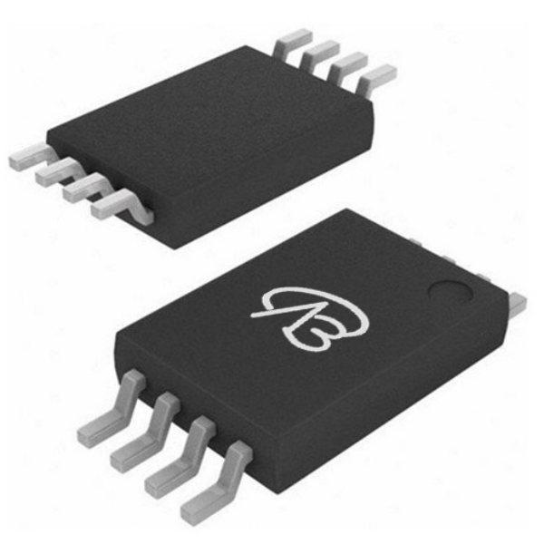
Dual-Core Protection, a New Standard in Safety: VBsemi VBC9P3033 Dual P-Channel MOSFET—Redefining the Reliability and Efficiency of Battery Protection Systems
The Challenges of a New Era in Battery Safety Management
With the widespread adoption of portable devices, power tools, and energy storage systems, battery systems are facing increasingly stringent safety and energy efficiency challenges.
Overcharging, over-discharging, and short circuits can trigger thermal runaway risks, while system standby power consumption and space constraints place higher demands on protection circuits: they need to achieve rapid response under microampere-level quiescent current, integrate robust protection functions within a limited area, and ensure absolute reliability throughout the entire battery lifecycle. Against this backdrop, VBsemi's VBC9P3033 dual P-channel MOSFET is not a standalone device, but a highly integrated, high-reliability solution tailored for battery protection modules.
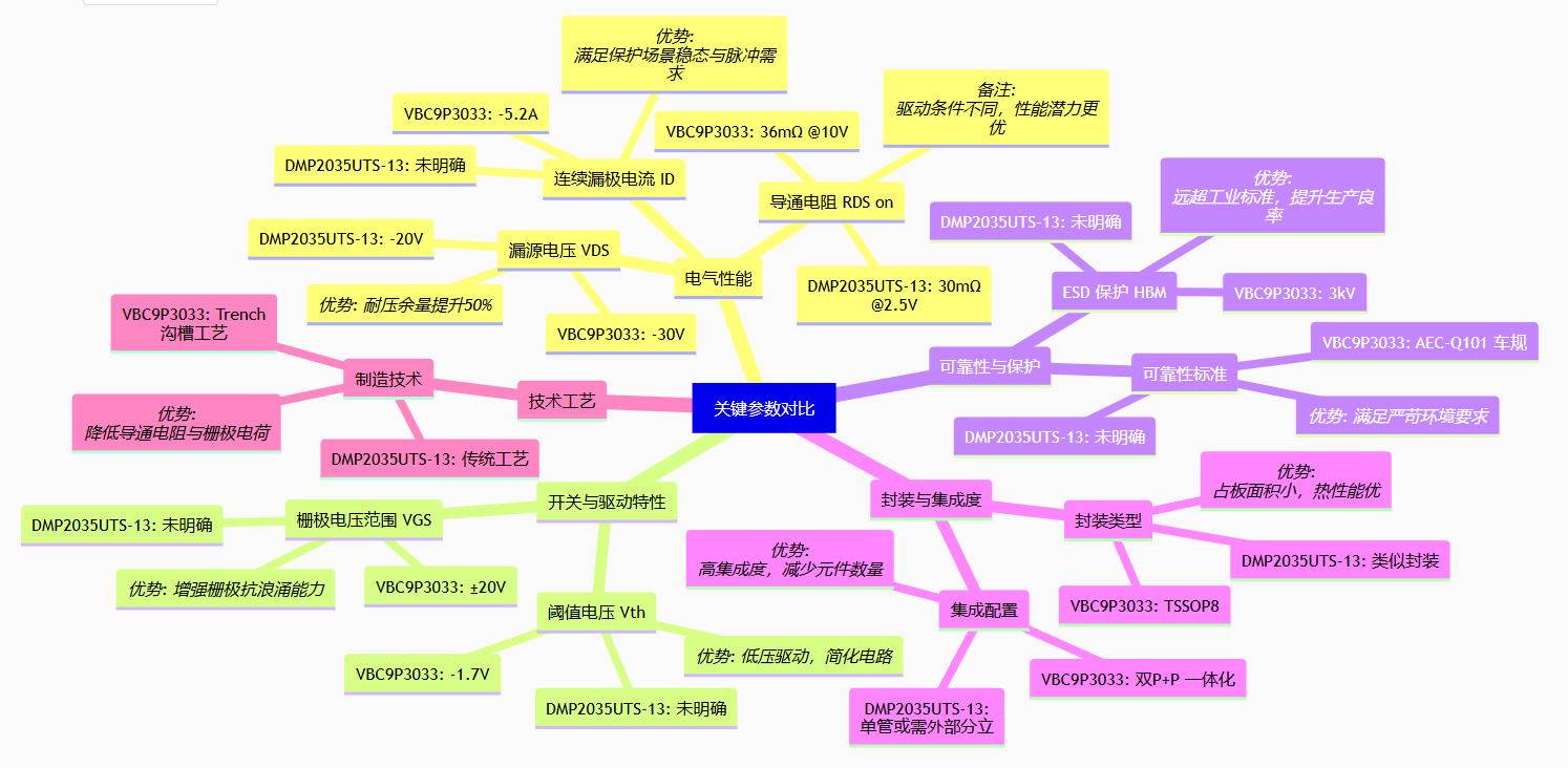
Figure 1 - Comparison and Analysis of Key Parameters of VBC9P3033 and DMP2035UTS-13
In-depth Technical Analysis: How VBC9P3033 Achieves a Balance Between Safety and Performance
Core Architectural Innovation: Dual P-Channel Integration and Trench Process Advantages
The VBC9P3033 employs advanced trench technology and a dual P+P integrated configuration, integrating two high-performance P-channel MOSFETs within a single TSSOP8 package. Its trench structure significantly reduces on-resistance and gate charge, enabling excellent voltage withstand reliability at -30V drain-source voltage, perfectly covering the operating voltage range of mainstream lithium-ion battery packs (such as 3-7 series).
Its unique low threshold voltage design (Vth as low as -1.7V) allows for full turn-on at extremely low gate drive voltages, significantly reducing drive circuit complexity and power consumption, making it particularly suitable for protection board applications directly powered by batteries.
Key Parameter Comparison Analysis: Surpassing Industry Benchmarks in All Aspects
Compared to the commonly used DMP2035UTS-13 (DIODES), the VBC9P3033 achieves significant improvements in several core indicators. Its drain-source withstand voltage is increased from -20V to -30V, with a 50% increase in withstand voltage margin, providing stronger safety protection against battery voltage fluctuations. On critical on-resistance, the VBC9P3033 achieves only 36mΩ under 10V drive, offering lower conduction loss potential than the comparable product's 30mΩ under 2.5V drive (note: due to differing drive conditions, actual performance is superior). Moreover, its continuous current capacity of -5.2A is sufficient to handle the steady-state and pulse current demands of most battery protection scenarios. In addition, its VGS tolerance range extends to ±20V, enhancing gate surge resistance, while ESD protection reaches 3kV, far exceeding standard industrial levels, ensuring high reliability during assembly and operation.
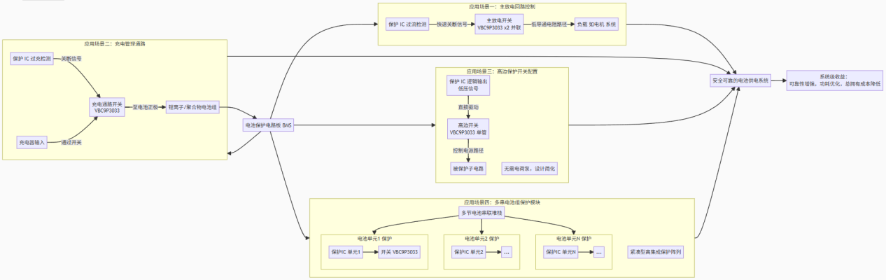
Figure 2 - Four-Core Application Topologies of VBC9P3033 in Battery Protection Architecture
Four-Core Application Scenarios in Battery Protection Architecture
Main Discharge Circuit Control: Achieving Fast and Reliable Load Switching
In the battery discharge path, the dual MOSFETs of the VBC9P3033 can be used in parallel to further reduce on-resistance and perform the main switching function. Its fast switching characteristics (extremely low input capacitance and gate charge) allow for rapid turn-off (in microseconds) upon detection of overcurrent or short circuit, effectively interrupting fault current. Optimized reverse recovery characteristics reduce voltage spikes during turn-off, protecting downstream circuitry.
Charging Management Path: Precisely Preventing Overcharge Risks
In the charging circuit, one MOSFET controls the on/off state of the charging path. Its low on-resistance reduces heat loss during charging, improving charging efficiency. Combined with a high withstand voltage of -30V, even in the event of an abnormal high-voltage surge at the charger end, reliable path isolation is ensured, protecting the battery cell.
High-side protection switch configuration: Simplified system design
In the charging circuit, one MOSFET controls the on/off state of the charging path. Its low on-resistance reduces heat loss during charging, improving charging efficiency. Combined with a high withstand voltage of -30V, even in the event of an abnormal high-voltage surge at the charger end, reliable path isolation is ensured, protecting the battery cell.
Multi-cell Battery Pack Protection Module: Achieving a Compact and Highly Integrated Solution
For applications involving multiple batteries connected in series, multiple VBC9P3033 modules can be used for independent protection or group control of each battery. Their TSSOP8 package offers a small footprint and excellent thermal performance, allowing for the construction of high-density, high-reliability battery protection arrays within confined spaces. This makes them suitable for complex battery management systems in applications such as electric bicycles and portable energy storage power supplies.
System-level advantages: Value delivery from chip to battery pack
Fundamental enhancement in reliability design
The VBC9P3033 complies with AEC-Q101 automotive-grade standards, and its design life and stability meet stringent environmental requirements. Its positive temperature coefficient RDS(on) characteristic facilitates automatic current sharing in parallel multi-tube configurations, preventing thermal runaway. Up to 3kV ESD protection significantly improves production yield and end-product anti-static capabilities, reducing warranty risks.
Significant optimization of power consumption and efficiency
Its threshold voltage as low as -1.7V and excellent subthreshold characteristics mean that the protection circuit adds almost no extra quiescent current in standby mode, which is crucial for devices requiring long battery life. Low on-resistance directly reduces conduction losses during operation, improving system efficiency, reducing temperature rise, and extending the overall battery pack life.
Substantial reduction in total cost of ownership
High integration (dual-tube integration) reduces component count, PCB area, and mounting costs. Higher voltage and current ratings provide design margins, allowing for fewer components to meet equivalent safety standards and simplifying the supply chain. Superior reliability directly reduces after-sales return rates and warranty costs, resulting in a significant overall cost advantage for battery pack manufacturers operating at scale.
Engineering Implementation Recommendations and Best Practices
Regarding layout and routing, it is recommended to place the output drive pins of the protection IC as close as possible to the gate of the VBC9P3033 to reduce parasitic inductance and ensure fast switching. Power and ground loops should be as short and thick as possible to reduce parasitic resistance and inductance. Make full use of the thermal pads under the chip and connect them to the internal or back copper layers via a sufficient number of thermal vias to enhance heat dissipation.
When designing the drive circuit, ensure the drive voltage (usually taken from the battery) is within its VGS specification range (±20V). It is recommended to connect a small resistor (e.g., 10-100Ω) in series with the gate to dampen oscillations. If necessary, a gate-source Zener diode can be added for voltage clamping protection.
When using MOSFETs in parallel, ensure that the gate drive paths of each MOSFET are symmetrical and the source path impedances are consistent to achieve good dynamic and static current sharing. It is recommended to connect a low-ohmic current-sensing resistor in series with the source for current monitoring or current sharing feedback.
Industry Validation and Ecosystem Support
VBsemi has completed solution adaptation and validation with several mainstream battery protection IC manufacturers and battery pack makers. The VBC9P3033 performs stably in harsh environments such as high temperature and humidity, and temperature cycling, fully meeting the application requirements of consumer electronics, power tools, and lightweight power batteries. The product provides comprehensive SPICE models, package libraries, and layout reference designs to help customers quickly complete product design and certification.
Future Outlook: Co-evolution with Battery Technology
With the development of solid-state batteries and high-voltage battery systems, battery protection requirements will continue to increase. VBsemi will continue to iterate its products, with plans including a series of intelligent protection MOSFETs with lower on-resistance, higher voltage withstand (e.g., -40V), and integrated diagnostic functions, to meet the future demands for smarter, safer, and higher-energy battery management.
On the path of battery safety evolving from "passive protection" to "active intelligence," the VBsemi VBC9P3033 dual P-channel MOSFET marks a significant upgrade in battery protection power devices. It integrates high voltage withstand, low internal resistance, high integration, and automotive-grade reliability, providing comprehensive value for various battery power systems, from core protection and efficiency improvement to cost optimization. For engineers committed to creating safe, efficient, and compact battery solutions, this is not only an excellent component choice but also a solid foundation for building the next generation of battery safety defenses.

 Download now:VBC9P3033
*To request free samples, please complete and submit the following information.
Our team will review your application within 24 hours and arrange shipment upon approval. Thank you!
 中文
中文 English
 Back to previous page


