 中文
 English

VBQA1308 MOSFET Replacement for AON6380: 24A and 80A Devices
 Back to previous page

The AON6380 front page lists 24 A and 6.8 mΩ maximum at 10 V gate drive. The replacement VBQA1308 lists 80 A and 0.007 Ω on its front page. Side by side, the replacement carries more than three times the current and a lower on-resistance.
These two parts are not in the same class. The original is a 24 A die with 26 W dissipation; the replacement is an 80 A die with 155 W, and both are marked DFN5×6. Junction-to-case thermal resistance differs by nearly eight times. The on-resistance row needs care as well: the 6.8 mΩ of the original is a guaranteed maximum, while 0.007 Ω of the replacement is a typical value with the maximum column blank. Compared at the same basis, the typical value of the replacement is 3 percent above the worst-case value of the original.
Gate charge shows the widest gap. The original gives 13 nC typical at 10 V drive; the replacement gives 61 nC in the same column, 3.7 times higher. In a high-frequency socket, this part raises drive loss noticeably.
Two different current classes
| Parameter | AON6380 | VBQA1308 |
|---|---|---|
| Package | DFN5×6 | DFN5×6 |
| Continuous drain current, TC 25 ℃ | 24 A | 80 A |
| Continuous drain current, TC 100 ℃ / 70 ℃ | 24 A at 100 ℃ | 60 A at 70 ℃ |
| Continuous drain current, TA 25 ℃ | 22 A | 50 A, 10 s |
| Pulsed drain current | 88 A | 210 A |
| Power dissipation, TC 25 ℃ | 26 W | 155 W |
| Junction-to-case | 3.8 typ / 4.8 max ℃/W | 0.5 typ / 0.6 max ℃/W |
| Junction temperature limit | 150 ℃ | 175 ℃ |
The original repeats 24 A at both 25 ℃ and 100 ℃ case temperature; a footnote states that this rating is package limited. The replacement reaches 80 A at 25 ℃ case, also package limited, and its footnotes give 90 A as the package ceiling. Neither case-temperature current represents the steady-state capability of the die on a board; both need thermal recalculation.
Dissipation and thermal resistance separate the two more clearly. 26 W against 155 W, and 3.8 ℃/W against 0.5 ℃/W junction-to-case. In the same DFN5×6 outline, the replacement has a much larger die and a lower thermal path through the exposed pad. The replacement can therefore serve high-current sockets where the original cannot, and in sockets the original already handles, the replacement runs with more margin.
On-resistance column and guarantee
| Parameter | AON6380 | VBQA1308 |
|---|---|---|
| RDS(on) at 10 V, typ / max | 5.6 / 6.8 mΩ | 7.0 mΩ / not listed |
| Test current at 10 V | 20 A | 30.8 A |
| RDS(on) at 4.5 V, typ / max | 8.2 / 10.5 mΩ | 9.0 mΩ / not listed |
| Test current at 4.5 V | 20 A | 27 A |
| RDS(on) at 125 ℃, 10 V, typ / max | 8.1 / 9.8 mΩ | not listed |
The original supplies both typical and maximum values at both gate voltages, and guarantees no more than 6.8 mΩ at 10 V. The replacement supplies only a typical value; the maximum column is blank.
Typical against typical: 7.0 mΩ against 5.6 mΩ, 25 percent higher. Typical of the replacement against maximum of the original: 7.0 against 6.8, 3 percent higher. The worst guaranteed unit of the original is still below the typical value of the replacement. This row gives the replacement no advantage.
Design values can only be built from the typical figure. At 10 V, 7.0 mΩ with a 20 percent margin becomes 8.4 mΩ, 24 percent above the 6.8 mΩ guarantee of the original. What the replacement lacks is a maximum limit; batch consistency has to be confirmed by measurement.
Test current also differs, 30.8 A for the replacement against 20 A for the original. A higher test current usually reads slightly higher resistance, which favours the original. A strict same-current comparison requires bench measurement.
Gate charge at each drive level
| Parameter | AON6380 | VBQA1308 |
|---|---|---|
| Total gate charge at 10 V, typ / max | 13 / 25 nC | 61 nC / not listed |
| Total gate charge at 4.5 V, typ / max | 6.2 / 12 nC | 31.5 nC / not listed |
| Gate-source charge | 2.2 nC | 10 nC |
| Gate-drain charge | 2.6 nC | 6 nC |
| Charge test current | 20 A | 30.8 A at 10 V |
| Charge test bus | 10 V | 15 V |
The front page of the replacement lists Qg 31 nC typical. That number belongs to the 4.5 V drive column, at 31.5 nC, not the 10 V column. At 10 V the datasheet gives 61 nC. Comparing 31 nC against the 10 V figure of the original understates the gap by half.
At 10 V: 61 nC against 13 nC, 3.7 times higher. At 4.5 V: 31.5 against 6.2, about 4 times higher. The original gives maximum values at both levels; the replacement gives a single figure for each.
Gate-drain charge is 6 nC against 2.6 nC, about 1.3 times higher. This term sets the length of the Miller plateau and drives the risk of spurious turn-on under dv/dt in bridge circuits.
At 200 kHz and 10 V drive, gate drive loss scales as Qg × VGS × f. The original at 13 nC is about 0.026 W; the replacement at 61 nC is about 0.122 W, a difference near 0.1 W per device. That is small for one device and scales with phase count and frequency.
Capacitance at a common bias
| Parameter | AON6380 | VBQA1308 |
|---|---|---|
| Input capacitance | 825 pF typ | 1180 pF, printed in max column |
| Output capacitance | 335 pF typ | 425 pF, printed in max column |
| Reverse transfer capacitance | 40 pF typ | 170 pF, printed in max column |
| Test condition | VGS = 0 V, VDS = 15 V, 1 MHz | VGS = 0 V, VDS = 15 V, 1 MHz |
All three capacitance rows share the same bias: gate shorted to source, drain at 15 V. They can be compared directly. The replacement is 43 percent higher on input capacitance, 27 percent higher on output capacitance, and 3.25 times higher on reverse transfer capacitance.
The replacement prints a single value in the maximum column for each of the three rows, with the typical column blank; the original gives typical values. The basis is not perfectly matched, but 170 pF against 40 pF remains a multiple even under the most generous reading.
Reverse transfer capacitance sets the Miller plateau and the sensitivity to dv/dt. In a half bridge or full bridge, dead time and gate turn-off resistance must be recalculated after the swap; the values of the original cannot be carried over.
Package and pinout
| Item | AON6380 | VBQA1308 |
|---|---|---|
| Package | DFN5×6 | DFN5×6 |
| Body size | 5.2 × 5.55 mm, vendor package page | 6.15 × 5.15 mm, datasheet |
| Thickness | 0.95 mm, vendor package page | not listed |
| Pins 1–3 | source | source |
| Pin 4 | gate | gate |
| Pins 5–8 | drain | drain |
| Exposed pad | drain | drain |
The pinout is identical: pins 1 to 3 source, pin 4 gate, pins 5 to 8 drain, exposed pad to drain. The parts drop onto a board in the same orientation without crossing traces.
The body dimensions are not the same. The vendor package page of the original lists 5.2 × 5.55 mm; the datasheet of the replacement lists 6.15 × 5.15 mm, with the long side on a different axis. The land pattern must follow the recommended drawing of the replacement and cannot be copied from the original DFN5×6 footprint. Use a reflow profile for leadless packages with a 260 ℃ peak.
Avalanche energy and its inductor
| Parameter | AON6380 | VBQA1308 |
|---|---|---|
| Single-pulse avalanche energy | 2 mJ | 95 mJ |
| Avalanche current | 60 A | 60 A |
| Inductor | 0.001 mH | 0.1 mH |
The two energy figures differ by 47 times, but the inductor differs by 100 times. Avalanche energy scales with inductance, so the test stress itself is not the same order. The numbers cannot be compared directly.
Avalanche current can be compared: both parts list 60 A. For a socket that absorbs inductive turn-off, the two are comparable on current; on energy, the test inductance has to be scaled to the actual circuit before any conclusion.
The replacement datasheet gives the full avalanche test condition; the original gives a single point at 0.001 mH. A rigorous energy calculation on the original lacks the curve data and needs measurement.
Switching times and drive conditions
| Parameter | AON6380 | VBQA1308 |
|---|---|---|
| Turn-on delay, typ / max | 2.6 / 5 ns | 18 / 27 ns |
| Rise time, typ / max | 3 / 5 ns | 11 / 17 ns |
| Turn-off delay, typ / max | 20 / 30 ns | 70 / 105 ns |
| Fall time, typ / max | 3 / 5 ns | 10 / 15 ns |
| Test bus | 10 V | 15 V |
| Test current | 20 A | 24 A |
| External gate resistor | 3 Ω | 1 Ω |
| Load resistor | 0.75 Ω | 0.625 Ω |
All four switching times of the replacement are longer, but the test conditions differ: the original used a 3 Ω gate resistor and a 10 V bus, the replacement 1 Ω and 15 V. A smaller gate resistor switches faster, so the replacement is slower despite the lighter gate drive. The difference comes from the die, not from the test setup.
This table should not be read as an absolute statement that the replacement switches slowly, but the direction is clear: its gate charge and reverse transfer capacitance are much larger, so the switching transition is longer. A same-board comparison requires both parts soldered and measured at the same current, bus, and gate resistance.
Three application cases
The first case is a socket above 20 A where the 24 A rating of the original is not enough. Use the replacement. Its 80 A case-temperature current, 155 W dissipation, and 0.5 ℃/W junction-to-case give an order of magnitude more margin. The cost is a new land pattern and a drive-loss recalculation.
The second case is a DC-DC converter below 24 A and above 200 kHz. Do not swap. The replacement has 3.7 times the gate charge and 3.25 times the reverse transfer capacitance; drive and switching losses rise at high frequency, and the original suits this socket better.
The third case is a load switch or battery-protection path below 24 A at low frequency. The swap works, provided the missing maximum limit is accepted. The typical resistance of the replacement is 3 percent above the worst case of the original, so the design value should be taken as 8.4 mΩ.
Full parameter comparison
| Parameter | AON6380 | VBQA1308 |
|---|---|---|
| Package | DFN5×6 | DFN5×6 |
| Channel | N | N |
| VDS | 30 V | 30 V |
| VGS | ±20 V | ±20 V |
| VGS(th), min / typ / max | 1.4 / 1.8 / 2.2 V | 0.5 / not listed / 2.0 V |
| RDS(on) 10 V, typ / max | 5.6 / 6.8 mΩ | 7.0 mΩ / not listed |
| RDS(on) 4.5 V, typ / max | 8.2 / 10.5 mΩ | 9.0 mΩ / not listed |
| Continuous current, TC 25 ℃ | 24 A | 80 A |
| Continuous current, TA 25 ℃ | 22 A | 50 A, 10 s |
| Pulsed current | 88 A | 210 A |
| Qg 10 V, typ / max | 13 / 25 nC | 61 nC / not listed |
| Qg 4.5 V, typ / max | 6.2 / 12 nC | 31.5 nC / not listed |
| Qgd | 2.6 nC | 6 nC |
| Ciss at 15 V | 825 pF | 1180 pF |
| Coss at 15 V | 335 pF | 425 pF |
| Crss at 15 V | 40 pF | 170 pF |
| td(on) / td(off) | 2.6 / 20 ns | 18 / 70 ns |
| Body diode VSD, typ / max | 0.7 / 1.0 V at 1 A | 0.8 / 1.2 V at 22 A |
| Trr / Qrr | 11 ns / 17 nC | 52 / 78 ns, 70.2 / 105 nC |
| Avalanche energy | 2 mJ, L = 0.001 mH | 95 mJ, L = 0.1 mH |
| RthJA, steady state | 45 typ / 55 max ℃/W | 90 ℃/W max |
| RthJC | 3.8 typ / 4.8 max ℃/W | 0.5 typ / 0.6 max ℃/W |
| Junction range | -55 to 150 ℃ | -55 to 175 ℃ |
Other parts in the same package family
VBGQA1606 is a 60 V N-channel part in the same package family, 60 A and 6.5 mΩ, using SGT technology. Where the bus stays under 48 V and more voltage headroom is needed, this part fits better than the 30 V class.
VBGQA1603 is another DFN5×6 60 V N-channel part, 90 A and 2.8 mΩ. Its current capability is close to the replacement and its voltage rating is twice as high. For a bus above 30 V, look at this part first.
Keeping the original is also a valid choice. If the design runs below 24 A and above 200 kHz, the low gate charge and low reverse transfer capacitance of the original are its advantages, and a swap forces a recalculation of drive and dead time. That part is positioned for low current and high frequency; the replacement is positioned for high current and low frequency. The two do not overlap.
Checks before the swap
- Land pattern: pinout matches, but body size differs, 5.2 × 5.55 mm for the original and 6.15 × 5.15 mm for the replacement. Redraw the footprint from the replacement drawing.
- Resistance: the replacement has only a typical value of 7.0 mΩ with the maximum blank. Take the design value as 8.4 mΩ, 24 percent above the 6.8 mΩ guarantee of the original.
- Gate charge: the 31 nC on the front page is the 4.5 V figure; the 10 V figure is 61 nC. Use 61 nC for a 10 V design.
- Capacitance: the replacement prints single values in the maximum column, while the original gives typical values. Reverse transfer capacitance is 170 pF against 40 pF.
- Current: both ratings are package limited. The replacement gives 50 A at 25 ℃ ambient for 10 s; steady state needs a 90 ℃/W recalculation.
- Thermal: junction-to-case is 0.5 ℃/W for the replacement against 3.8 ℃/W for the original. A heatsinked socket sees much less drop through the replacement.
- Avalanche: both list 60 A avalanche current, but the test inductors differ by 100 times, so the energy figures cannot be compared directly.
- Threshold: 0.5 to 2.0 V for the replacement against 1.4 to 2.2 V for the original. The lower limit needs a check that gate turn-off does not cause spurious conduction.
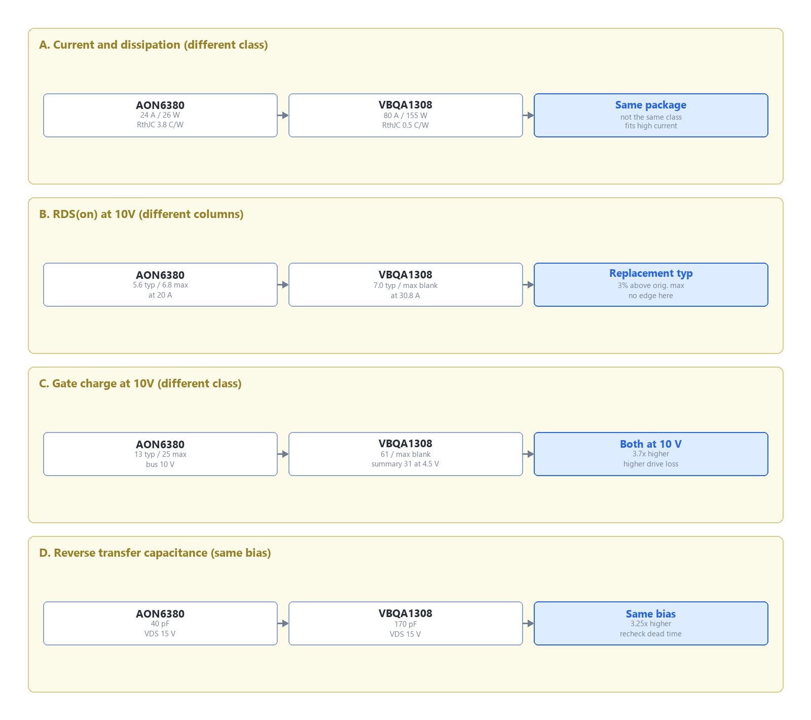
Figure 1. Six datasheet rows side by side. Current and dissipation: 24 A and 26 W for the original against 80 A and 155 W for the replacement. RDS(on) at 10 V: 5.6 typ / 6.8 max mΩ for the original against 7.0 mΩ typ with the maximum blank. Gate charge at 10 V: 13 nC typ for the original against 61 nC. Reverse transfer capacitance: 40 pF against 170 pF. Junction-to-case: 3.8 ℃/W against 0.5 ℃/W.
Frequently asked questions
Do the two parts share a pinout?
Yes. Both use pins 1 to 3 for source, pin 4 for gate, pins 5 to 8 for drain, and the exposed pad for drain. Body size differs, so the land pattern must be redrawn for the replacement.
The replacement lists 80 A against 24 A. Is this an upgrade?
It is a different class of device. The replacement has a larger die, 155 W dissipation, and 0.5 ℃/W junction-to-case; the original has 26 W and 3.8 ℃/W. For high current the replacement wins; below 24 A at high frequency the original is the better fit.
The replacement shows 0.007 Ω against 0.0068 Ω. Is it lower?
Not in the same column. The 6.8 mΩ of the original is a maximum; 0.007 Ω of the replacement is typical with the maximum blank. The typical value of the replacement is 3 percent above the maximum of the original.
The front page says Qg 31 nC but the table says 61 nC. Which applies?
31 nC is the 4.5 V drive figure; 61 nC is the 10 V figure. For a 10 V design, use 61 nC.
What does 170 pF against 40 pF reverse transfer capacitance change?
It changes the Miller plateau length and the risk of spurious turn-on under dv/dt. In a bridge circuit, dead time and gate turn-off resistance must be recalculated.
Is the replacement much stronger on avalanche energy, 2 mJ against 95 mJ?
The test inductors differ, 0.001 mH for the original and 0.1 mH for the replacement, and energy scales with inductance. The figures cannot be compared directly. Avalanche current can be compared, and both list 60 A.
The replacement threshold goes down to 0.5 V. Could it turn on by itself?
That is lower than the 1.4 V of the original. Confirm that gate turn-off can pull low enough, especially at high dv/dt, where reverse transfer capacitance couples drain transients onto the gate.

Download PDF document
 Download now


