 中文
 English

Scenario Product Guide
48V Servo Drive MOSFET Selection: Braking and PWM Losses
 Back to previous page

A 1 kW 48V industrial servo drive carries about 20A rms per phase, and at 16 kHz carrier each of the six bridge devices dissipates roughly 0.49W in conduction against 0.44W in switching — the two terms are the same size, which is true at no other common bus voltage. This applies to 48V DC-bus drives with a 60–65V regenerative braking clamp, natural or forced convection inside a cabinet, and 8/16 kHz space-vector modulation. Below about 8 kHz conduction dominates and RDS(on) alone is enough to choose; above roughly 24 kHz, or once the bus moves to 400V, gate charge becomes the first-order parameter and the ranking used here no longer applies.
At a glance
- The bus does not run at 48V. Regenerative braking pumps it to a 60–65V clamp, so the voltage class is 100V and a 60V device is already at its limit before the first deceleration.
- 48V is the one bus voltage where conduction and switching loss are comparable, so RDS(on) × Qg — not the headline on-resistance — is the selection metric at 16 kHz.
- VBsemi's 100V class lists 123 parts but only one in LFPAK56 (VBGED1103, 3.0 mΩ / 180A); the other eight surface-mount 100V parts are DFN8(5×6), so the package decision is made by the thermal path on your board, not by a wider choice.
Why a 48V servo is not a low-voltage copy of a 400V drive
In a 400V drive the switching term owns the design. Take the standard expression 0.5·V·I·(t<sub>r</sub>+t<sub>f</sub>)·f with 400V, 28A peak, 40 ns and 16 kHz: it comes to 1.79W per device, while conduction through 3 mΩ at the same current is 0.49W. The ratio is 3.6 to 1, so designers buy the fastest gate they can afford and tolerate a higher RDS(on). At 18V the same arithmetic inverts completely — switching drops to 0.08W and conduction is six times larger — which is why battery tool designs ignore gate charge. A 48V bus sits exactly between the two regimes, and that is the part most selection guides skip: at 16 kHz the two terms land within 12% of each other, so a part chosen purely for low RDS(on) can end up hotter than a slightly more resistive part with half the gate charge.
The second thing that changes at 48V is what the bus does when the motor is not motoring. A servo decelerates as often as it accelerates, and every deceleration pushes energy back through the bridge body diodes into the DC link. With no place to put it, the bus rises until something absorbs it — in practice a chopper switch and a dump resistor, clamped at 60–65V. That clamp, not the nominal 48V, is the voltage the semiconductors must survive, and it is the single most common reason a 60V part fails in a drive that measured perfectly on the bench.
What each design variable decides
| Design variable | Range in a 1 kW servo drive | What it decides | Device class |
|---|---|---|---|
| Nominal bus | 48V (12S–13S pack, or 48V PSU) | Nothing directly — the clamp does | — |
| Braking clamp | 60–65V trip, plus ring | Voltage class and margin | 100V (60V unfit, 80V marginal) |
| Phase current | 20A rms, 28A peak | Conduction loss, die area | RDS(on) ≤ 3.5 mΩ |
| Carrier frequency | 8 kHz standard, 16 kHz quiet | Gate charge, dead time, driver loss | Qg < 45 nC at 16 kHz |
| Ambient | 55°C cabinet air, 70°C hot spot | Package and copper area | LFPAK56 or DFN8 on 250 mm² |
| Braking duty | 1–5% average, seconds at a time | Thermal impedance, not RDS(on) | Small die is acceptable |
| Dead time | 0.5–1.5 µs at 16 kHz | Body-diode conduction window | Low Qrr, soft recovery |
The table is ordered by how much the variable moves the answer, not by voltage. The braking clamp is first because it eliminates an entire voltage class: 60V parts fail outright, 80V parts leave only 1.23× margin against a 65V clamp, and 100V is the first class that gives a believable 1.5× even with a 5V ring on top.
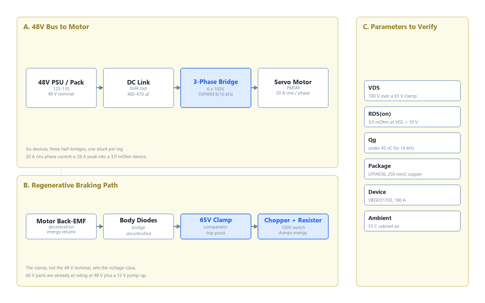
Figure 1: the 48V power path in a servo drive, with the regenerative braking clamp shown as a separate branch. The clamp, not the 48V nominal, sets the 100V device class.
Parameter comparison
Five parts, all N-channel, ratings taken from each published datasheet.
| Model | VDSS | ID | RDS(on) | Package | Position in this design |
|---|---|---|---|---|---|
| VBGED1103 | 100V | 180A | 3.0 mΩ @10V | LFPAK56 | Three-phase bridge, main choice |
| VBGQA1103 | 100V | 135A | 3.45 mΩ @10V | DFN8(5×6) | Bridge on a compact single-sided board |
| VBGQA1105 | 100V | 105A | 5.6 mΩ @10V | DFN8(5×6) | Lower-current axis, 10A class |
| VBGQA1107 | 100V | 75A | 7.4 mΩ @10V | DFN8(5×6) | Braking chopper, pulsing duty |
| VBGED1401 | 40V | 250A | 0.7 mΩ @10V | LFPAK56 | 24V brake release and control-rail switch |
The catalogue fact that no comparison page will give you: the 100V class in VBsemi's published selector holds 123 part numbers, and exactly one of them is in LFPAK56. The other eight surface-mount 100V parts are DFN8(5×6), and the lowest on-resistance in that group is 3.45 mΩ against 3.0 mΩ for the LFPAK56 part. So "which 100V part" is not a five-way comparison — it is a single part, and the real engineering decision is whether 250 mm² of drain copper under a DFN8 is enough to give up the clip-bond thermal path of the larger package.
Engineering trade-offs: conduction, switching and the braking path
Conduction averages 0.49W per device, and the averaging factor matters. A 20A rms phase current is 28A peak, and a device conducts for roughly half of each carrier period with a modulation-dependent duty. Using the standard loss integral over a sinusoidal modulation index of 0.9 and a power factor of 0.85, the conduction term works out to I<sub>peak</sub>² · RDS(on) · 0.206. At 3.0 mΩ that is 0.49W; summed over six devices it is 2.9W, or 0.3% of the 1 kW output. Anyone who multiplies 20A² by 3 mΩ and gets 1.2W has forgotten that the device is not conducting continuously, and will over-size the whole bridge by a factor of two.
Switching is the term that catches people at 48V. At 16 kHz with 40 ns of combined rise and fall, the per-device switching loss is 0.44W — within 12% of conduction. Move to an 8 kHz carrier and it halves to 0.22W, which is why drives that accept the audible tone can use a slower, cheaper gate drive. The crossover is the design lever: if the mechanical design forces 16 kHz, the part has to be chosen on RDS(on) × Qg, and a 3.45 mΩ device with 30 nC can beat a 3.0 mΩ device with 55 nC in the same footprint.
The braking chopper is a thermal-impedance problem, not a resistance problem. During a deceleration from full speed the regen current can match the motoring current for a few hundred milliseconds, then it stops for seconds. A 7.4 mΩ device handling 20A pulses dissipates 3W during the pulse, but the junction never reaches steady state because the pulse is short relative to the package thermal time constant. This is the one position where a small die is the right answer: VBGQA1107 at 100V and 7.4 mΩ is cheaper and physically smaller than the phase-leg part, and its transient thermal impedance is what the design must be checked against.
The 40V part is not a compromise, it is a different rail. The brake release solenoid, the fan, and the 24V control supply are all single-digit-ampere loads that never see the 65V clamp. Putting a 100V device there wastes die area and gate charge: VBGED1401 at 40V and 0.7 mΩ carries 5A with 17 mW of conduction loss, and its gate charge is small enough for a simple driver.
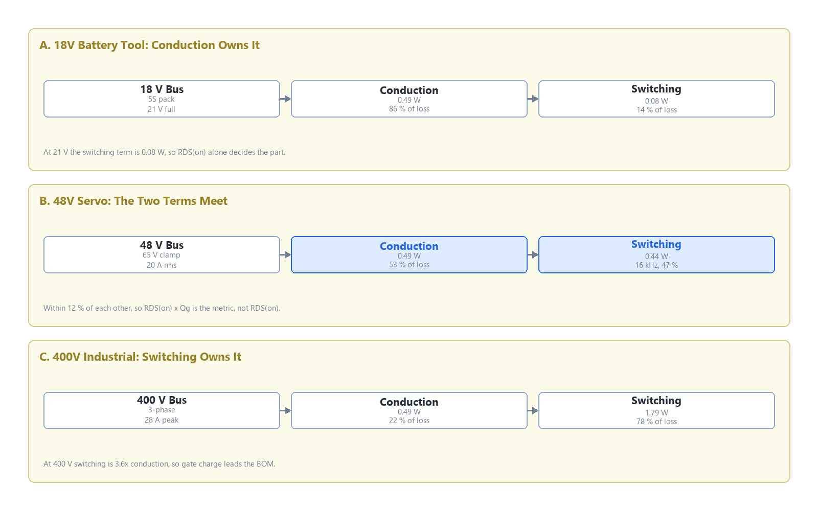
Figure 2: conduction against switching at the same 20A phase current across three bus voltages. At 18V conduction owns the budget, at 48V the two terms meet, and at 400V switching is 3.6 times conduction.
Four field mistakes
- Sizing the bridge on the 48V nominal bus. A 60V part has 1.25× margin at 48V and 0.92× at the 65V clamp, so it is already over its rating during the first hard stop. The number to design against is the clamp plus the inductive ring, not the supply voltage printed on the label.
- Choosing on RDS(on) alone at 16 kHz. The 3.0 mΩ part and the 3.45 mΩ part differ by 0.07W per device in conduction, which is less than the switching difference between a 30 nC and a 55 nC gate. A BOM that picks the lower resistance and ignores gate charge can come out 0.5W hotter per bridge.
- Giving the braking chopper the same part as the phase legs. It works thermally, but it doubles the cost of a position that conducts 1–5% of the time. Worse, a designer who sizes it for steady-state 20A will pick a part three times larger than the pulse duty requires.
- Ignoring the dead-time window at 16 kHz. With a 1 µs dead time at 16 kHz, the body diode conducts for 1.6% of every period. In a 100V MOSFET that is a real loss and a real recovery charge, and a part with poor Qrr will run hotter in the diode than in the channel.
Where this approach stops working
Push the carrier above 24 kHz and switching loss overtakes conduction even at 48V, at which point gate charge dominates and a device with 20% higher RDS(on) but half the Qg wins. Above roughly 3 kW on a 48V bus the phase current passes 60A and two devices must be paralleled per switch, which makes current sharing and layout the design instead of the datasheet. If the drive has to survive a 2 kV surge without an external clamp, the 48V class is the wrong conversation entirely — that is a 400V bus with a different stack. And if the braking energy is large enough to need continuous dissipation, the chopper stops being a pulse device and becomes a steady-state thermal design that belongs on a heatsink, not on 250 mm² of copper.
FAQ
Q: Can a 60V MOSFET be used on a 48V servo bus?
A: No. The bus is clamped at 60–65V during regenerative braking, so a 60V device sits at or beyond its rating every time the axis decelerates. 100V is the practical floor.
Q: Why not 80V, which is cheaper than 100V?
A: Against a 65V clamp, 80V leaves 1.23× margin, which a 5V inductive ring plus a 10% supply tolerance consumes entirely. 100V gives 1.54× and is the first class that survives a hard stop without a TVS.
Q: Does the braking chopper really need a 100V part?
A: Yes, and it needs it more than the phase legs do — the chopper is the device that clamps the bus, so it sees the full 65V plus the ring on every pulse. Its die can be small, but its voltage class cannot.
Q: At what carrier frequency does gate charge start to matter?
A: Around 12–16 kHz. Below 8 kHz conduction is three to four times the switching term, so RDS(on) alone is a fair proxy; by 16 kHz they are equal, and above 24 kHz Qg is the dominant parameter.
Q: How much copper does a DFN8(5×6) need in a servo drive?
A: About 250 mm² of drain copper with via stitching into the inner layers, assuming 55°C cabinet air. Below 150 mm² the junction temperature is set by the footprint rather than by the silicon, and the 3.45 mΩ advantage over LFPAK56 disappears.

Download PDF document
 Download now:VBGED1103


Request Free Samples
*To request free samples, please complete and submit the following information.
Our team will review your application within 24 hours and arrange shipment upon approval. Thank you!