 中文
中文 English
Scenario Product Guide
VBsemi VBQF1310 Trench MOS: Balance Efficiency & Density for Compact AI PSU
 Back to previous page
.png)
New Power Supply Challenges in the Era of Decentralized AI Computing Power
As artificial intelligence extends from the cloud to the edge, compact AI servers, edge computing nodes, and accelerator cards face rigorous power supply design challenges.
Designing within limited board space requires accommodating the sudden power surges associated with high-performance acceleration units—such as GPUs and ASICs—while strictly controlling temperature rise and power loss. This necessitates high levels of integration regarding the efficiency, power density, and reliability of power components.
Against this backdrop, the VBQF1310 Trench MOSFET from VBsemi—featuring an ultra-thin DFN8 3x3 package and optimized electrical performance—emerges as an ideal choice for high-density, high-efficiency AI edge power supply solutions.
Technology Focus: How the VBQF1310 Achieves High-Efficiency Power Conversion in Compact Spaces
Key Structural Advantages: Synergy Between Trench Technology and Advanced Packaging
The VBQF1310 utilizes mature trench-gate technology combined with a low-profile DFN8 3x3 package, delivering excellent current-carrying and thermal dissipation capabilities within a compact footprint.Its trench structure effectively reduces on-resistance, while the large exposed pad on the bottom of the package ensures an efficient dual-sided heat dissipation path. This makes it particularly suitable for mounting on the back of a PCB or in confined spaces, offering greater flexibility for power delivery layouts in high-density AI acceleration modules.
Benchmarking Analysis of Key Parameters: Achieving Leading Performance within a Compact Footprint
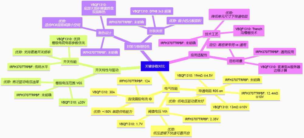
Compared to Infineon's IRFH3707TRPBF, the VBQF1310 demonstrates advantages across several key metrics that make it better suited for AI edge servers.Its continuous drain current reaches 30A—2.5 times that of the 12A benchmark model—significantly enhancing single-rail power delivery capability. The threshold voltage (Vth) is 1.7V—lower than the benchmark's 2.35V—ensuring rapid and reliable turn-on with low-voltage logic signals. Despite its ultra-compact package size, the optimized combination of power handling capability and on-resistance lays a solid foundation for high-switching-frequency, high-current-density applications.
Core application scenarios in compact AI servers
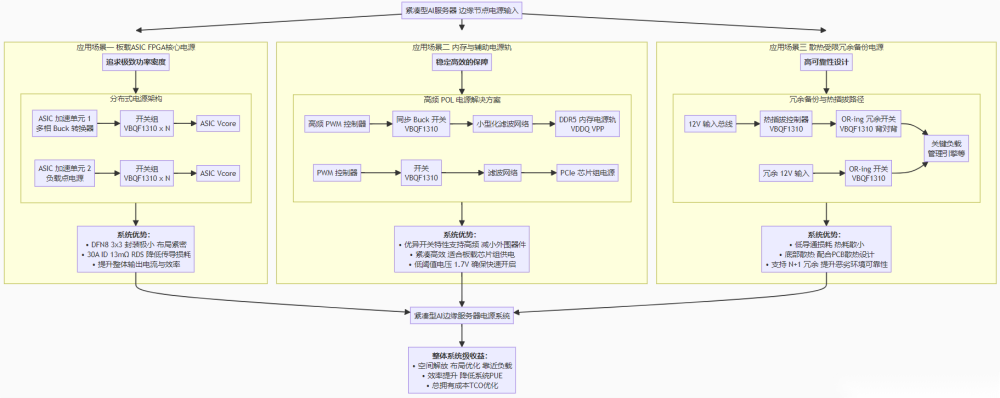
On-board ASIC/FPGA Core Power: Pursuing Ultimate Power Density
In edge AI inference cards or compact servers, distributed power architectures supplying multiple ASICs or FPGAs demand extremely high power density. The VBQF1310, housed in a tiny DFN8 3x3 package, enables power designers to place multiphase buck converters or point-of-load (POL) power supplies in closer proximity to the chips. With an RDS(on) as low as 13mΩ and a 30A current capability, it effectively minimizes conduction losses in each power phase, delivering higher overall output current and efficiency within a limited footprint.
Memory and Auxiliary Power Rails: A Guarantee of Stability and Efficiency
As the power consumption of DDR5 memory and high-speed interfaces rises, their power supply solutions require both high efficiency and a compact footprint. VBQF1310’s excellent switching characteristics, as reflected by its gate charge and capacitance parameters, help enable higher switching frequencies, thereby reducing the size of external inductors and capacitors. It is very well suited to provide a compact, efficient POL power solution for memory, PCIe slots, and other onboard chipsets.
Redundant Backup Power Supply for Thermally Constrained Environments
In highly integrated 1U or edge servers, space for heat dissipation is extremely limited. The low conduction loss of the VBQF1310 translates directly into reduced heat dissipation; combined with PCB thermal design, its package's thermal resistance characteristics enable stable operation without relying on forced-air cooling. This enhances system reliability in harsh environments while supporting essential power redundancy designs.
System-level value: Small size, significant contribution
Space Liberation and Layout Optimization
The ultra-compact package of the VBQF1310 frees up valuable routing space on AI server motherboards, allowing power circuitry to be placed closer to the load; this reduces parasitic inductance and improves dynamic response. Its bottom-side thermal design enables heat dissipation through the PCB's internal layers or backside, simplifying system-level thermal management.
Efficiency Improvement and Reduced Heat Dissipation
In typical multiphase buck circuits, the use of the VBQF1310 significantly reduces both switching and conduction losses. Its lower threshold voltage and optimized gate characteristics enhance driving efficiency—particularly under light-load conditions—thereby contributing positively to overall system energy efficiency and directly helping to lower the PUE of edge data centers.
Total Cost of Ownership Optimization
For large-scale deployments of edge AI nodes, every watt of power saved is significant. The VBQF1310 directly reduces operational electricity costs by enhancing power conversion efficiency. Its high reliability minimizes maintenance requirements, while its high power density enables the integration of more compute units onto a single server or accelerator card, thereby improving the return on investment for infrastructure.
Implementation and Design Recommendations
Layout and Thermal Design: It is recommended to place the VBQF1310 in an area of the PCB with good thermal connectivity, utilizing via arrays to conduct heat to internal copper layers or a heatsink on the backside. The drive loop should be kept as short as possible to minimize the impact of parasitic inductance on switching performance.
Gate Driving and Parallel Operation: The ±20V VGS range offers a wide selection of gate drive voltages. For high-current applications, multiple devices can be easily connected in parallel; thanks to consistent device parameters, achieving balanced current sharing is straightforward. It is recommended to include a small sense resistor at the source terminal to facilitate precise current monitoring and current-sharing control.
Reliability Verification and Ecosystem Compatibility
The VBQF1310 has undergone rigorous reliability testing and meets standards for industrial-grade and server applications. Its pinout and package are compatible with mainstream market models, facilitating rapid upgrades and replacements for existing designs. VBsemi offers comprehensive technical support—including simulation models, thermal analysis data, and reference designs—to help customers accelerate their time-to-market.
Future Outlook: Evolving Alongside Edge AI
To meet the rigorous demands for power efficiency, compact size, and high performance in edge AI devices, VBsemi will continue to optimize the VBQF1310 series. Future initiatives include lowering RDS(on) through process upgrades and exploring smart power module configurations—such as integrating driver or protection functions—to address the need for higher integration and intelligence in power management for next-generation edge AI servers.
In an era where AI computing power is ubiquitous, the VBsemi VBQF1310 Trench MOSFET offers a critical solution for power system design in compact AI servers and edge computing devices, combining high current capability and low power loss within an ultra-small package. It serves not only as a component for enhancing power density but also as a vital foundation for the efficient and reliable operation of edge AI devices.

Download PDF document
 Download now:VBQF1310


Request Free Samples
*To request free samples, please complete and submit the following information.
Our team will review your application within 24 hours and arrange shipment upon approval. Thank you!