 中文
中文 English
STC5DNF30V-VB Product details
 Back to previous page
Product introduction:
**Are you designing a compact power module where PCB area is limited, yet you need to manage two power paths simultaneously? Traditional solutions often require multiple discrete MOS transistors, which take up space and increase routing complexity. VBsemi STC5DNF30V-VB is designed for this exact challenge—it integrates two low-voltage N-channel MOSFETs in a TSSOP8 package, achieving a minimum on-resistance of 11mΩ with 20V withstand voltage and 7.5A current capability, making high-density dual-channel switch design simple and efficient.**
File download

Download PDF document
 Download now
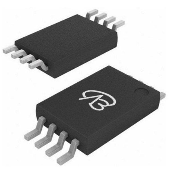
Product parameter:
| VB Package | Configuration | VDS(V) | VGS | Vthyp(V) | ID(A) | Rds2.5 | Rds4.5 | Rds10 | Technology |
|---|---|---|---|---|---|---|---|---|---|
| TSSOP8 | Dual-N+N | 20V | 0.86V | 7.5A | 17(mΩ) | 12(mΩ) | 11(mΩ) | Trench |
| VB Package | Configuration | VCE | VGE | VGEth(V) | VCEsat15V | ICE | Technology |
|---|---|---|---|---|---|---|---|
| TSSOP8 | Dual-N+N | Trench |
| VB Package | Configuration | VDS(V) | VGS | Vthyp(V) | ID(A) | Rds18 | Technology |
|---|---|---|---|---|---|---|---|
| TSSOP8 | Dual-N+N | 20V | 0.86V | 7.5A | Trench |
| VB Package | Configuration | VDS(V) | VGS | Vthyp(V) | ID(A) | Rds6 | Technology |
|---|---|---|---|---|---|---|---|
| TSSOP8 | Dual-N+N | 20V | 0.86V | 7.5A | Trench |
| VB Package | Polarity | Vz / VR | Pd | VF | IF | IR | Cd | Type |
|---|---|---|---|---|---|---|---|---|
| TSSOP8 | Dual-N+N | MOS |
- Voltage 20V, suitable for low-voltage power switching and load management
- Dual N+N configuration, one chip completes two independent controls
- Gate drive range ±12V, compatible with 2.5V~10V logic levels
- Threshold voltage 0.86V, reliable turn-on with low-voltage drive
- On-Resistance: 17mΩ (2.5V drive), 12mΩ (4.5V drive), 11mΩ (10V drive), low losses, minimal heat
- Maximum continuous drain current 7.5A, small package can handle high current
- Trench technology, excellent switching performance
**
Domain and module applications:
- **Lithium Battery Protection Board** – Dual-channel structure suitable for positive and negative terminal dual protection. Microsecond shutdown capability effectively prevents overcharge, over-discharge, and short circuit damage.
- **DC-DC Synchronous Rectification** – Dual N+N transistors replace two discrete MOS transistors, reducing conduction losses and improving conversion efficiency in buck-boost topologies.
- **Load Switches / Power Path Management** – Achieves independent on/off control for two paths in 5V/12V systems, saving PCB area and reducing standby power consumption.
- **Mobile Device Fast Charging Interface** – Utilizes 2.5V low drive capability, working with charging protocol chips for power switching and OVP protection.
- **Motor Drives / Power Tools** – Low RDS(on) reduces heat generation, supports 7.5A peak current, suitable for small DC motor speed control.
- **Industrial Sensors and PLC Modules** – Dual-channel serial control simplifies power distribution circuit design, improving system reliability.
- **Type-C Docking Stations / USB Hubs** – Precisely manages multiple VBUS power supplies, ensuring hot-swap safety and reducing voltage drop.
**One-sentence summary: STC5DNF30V-VB is not just a simple integration of two MOS transistors; it is the 'dual-channel efficiency expert' for low-voltage power supply designs, making your product smaller, cooler, and more reliable.**
* Please note: the above is only an example application scenario, the specific application depends on the requirements and conditions of the system design. When using this device, consult its data sheet for detailed technical specifications and features
Technical support:
* If you have any questions about the product, please fill out the form to submit, we will reply you within 24 hours


