 中文
中文 English
FDW2503NZ-VB Product details
 Back to previous page
Product introduction:
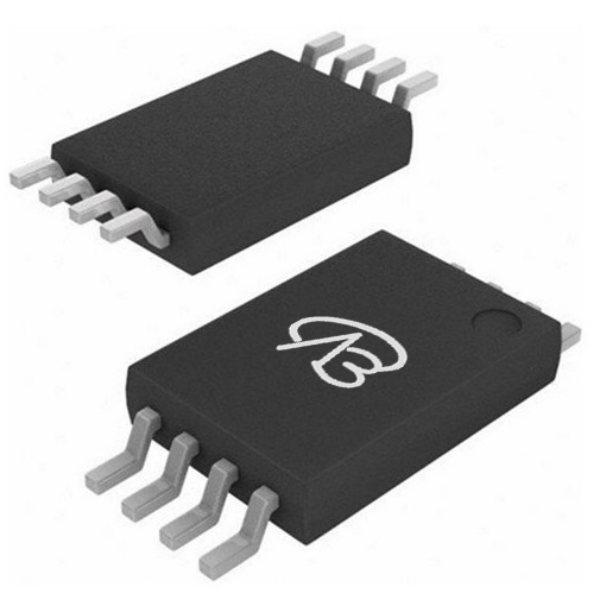
**Are you designing a high-density power module or a compact battery management system where PCB area is at a premium, yet you need to handle dual power paths simultaneously? Traditional discrete MOS transistors not only take up space but can also introduce additional routing losses. VBsemi FDW2503NZ-VB is designed for this exact challenge—it integrates two N+N channel MOSFETs in a TSSOP8 small package, combining 20V withstand voltage, 7.5A continuous current capability, and a minimum on-resistance of 11mΩ into one device, making dual-channel low-loss switching design unprecedentedly simple and efficient.**
File download

Download PDF document
 Download now
Product parameter:
| VB Package | Configuration | VDS(V) | VGS | Vthyp(V) | ID(A) | Rds2.5 | Rds4.5 | Rds10 | Technology |
|---|---|---|---|---|---|---|---|---|---|
| TSSOP8 | Dual-N+N | 20V | 0.86V | 7.5A | 17(mΩ) | 12(mΩ) | 11(mΩ) | Trench |
| VB Package | Configuration | VCE | VGE | VGEth(V) | VCEsat15V | ICE | Technology |
|---|---|---|---|---|---|---|---|
| TSSOP8 | Dual-N+N | Trench |
| VB Package | Configuration | VDS(V) | VGS | Vthyp(V) | ID(A) | Rds18 | Technology |
|---|---|---|---|---|---|---|---|
| TSSOP8 | Dual-N+N | 20V | 0.86V | 7.5A | Trench |
| VB Package | Configuration | VDS(V) | VGS | Vthyp(V) | ID(A) | Rds6 | Technology |
|---|---|---|---|---|---|---|---|
| TSSOP8 | Dual-N+N | 20V | 0.86V | 7.5A | Trench |
| VB Package | Polarity | Vz / VR | Pd | VF | IF | IR | Cd | Type |
|---|---|---|---|---|---|---|---|---|
| TSSOP8 | Dual-N+N | MOS |
- Drain-Source Voltage VDS: 20V, suitable for low-voltage battery and load management scenarios
- Gate-Source Voltage VGS: ±12V, compatible with common low-voltage logic drives
- Threshold Voltage Vth: 0.86V, can be turned on at low voltage, supporting low-voltage direct drive
- On-Resistance RDS(on): 17mΩ @ VGS=2.5V; 12mΩ @ VGS=4.5V; 11mΩ @ VGS=10V
- Continuous Drain Current ID: 7.5A, small package carrying high current
- Package Type: TSSOP8, Dual N+N configuration, saves PCB area
- Technology: Trench process, excellent figure of merit
**
Domain and module applications:
- **Lithium Battery Protection Board** – Dual N-channel series structure suitable for charge/discharge circuit control. Low on-resistance reduces thermal losses, extending battery life.
- **DC-DC Buck/Boost Modules** – Used as low-side/high-side switches in synchronous rectification topologies, improving conversion efficiency and allowing smaller inductor sizes.
- **Load Switches and Power Path Management** – TSSOP8 dual-channel integration, suitable for multi-rail power switching in portable devices, enabling compact and low-cost power distribution.
- **Portable Device Charging Circuits** – Suitable for 5V or 12V input. Low threshold characteristic allows direct drive by MCU I/O or logic levels.
- **Power Tools/Small Appliance Motor Drives** – Dual channels can be used for half-bridge or H-bridge low-speed control, simplifying board layout and reducing parasitic parameters.
- **Type-C Interfaces and USB Hubs** – Used for VBUS on/off control. Low conduction voltage drop ensures high-current transmission without overheating.
**One-sentence summary: FDW2503NZ-VB is not just an ordinary dual-channel MOS transistor; it is the 'dual-channel integration expert' and 'thermal loss terminator' for your low-voltage, small-size, high-efficiency power supply designs.**
* Please note: the above is only an example application scenario, the specific application depends on the requirements and conditions of the system design. When using this device, consult its data sheet for detailed technical specifications and features
Technical support:
* If you have any questions about the product, please fill out the form to submit, we will reply you within 24 hours


