 中文
中文 English
SI6954ADQ-T1-BE3-VB Product details
 Back to previous page
Product introduction:
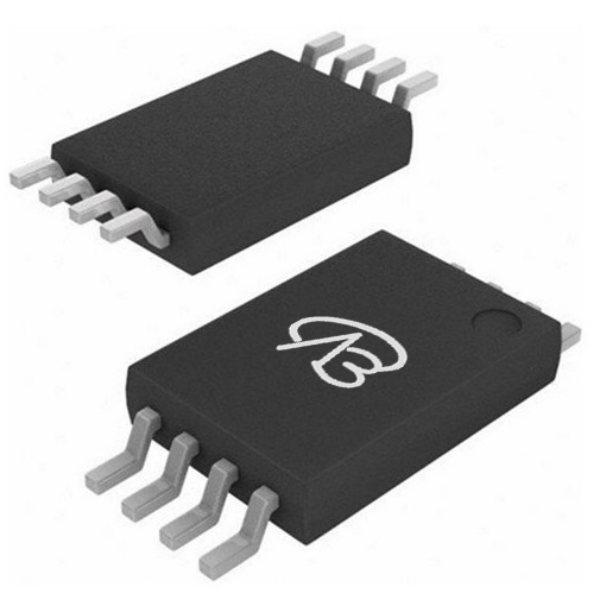
**VBsemi SI6954ADQ-T1-BE3-VB is a Dual N+N channel field-effect transistor manufactured using Trench technology, designed for low-voltage, high-efficiency power conversion and precision load control scenarios. Its TSSOP8 small package integrates two MOSFETs within a limited board area, facilitating the implementation of topologies such as synchronous rectification and half-bridge drivers, significantly enhancing power density and layout flexibility. The device supports a 20V drain-source voltage, and its gate drive is compatible with 2.5V/4.5V logic levels, adapting to low-voltage digital control interfaces and simplifying system design.**
File download

Download PDF document
 Download now
Product parameter:
| VB Package | Configuration | VDS(V) | VGS | Vthyp(V) | ID(A) | Rds2.5 | Rds4.5 | Rds10 | Technology |
|---|---|---|---|---|---|---|---|---|---|
| TSSOP8 | Dual-N+N | 20V | 0.86V | 7.5A | 17(mΩ) | 12(mΩ) | 11(mΩ) | Trench |
| VB Package | Configuration | VCE | VGE | VGEth(V) | VCEsat15V | ICE | Technology |
|---|---|---|---|---|---|---|---|
| TSSOP8 | Dual-N+N | Trench |
| VB Package | Configuration | VDS(V) | VGS | Vthyp(V) | ID(A) | Rds18 | Technology |
|---|---|---|---|---|---|---|---|
| TSSOP8 | Dual-N+N | 20V | 0.86V | 7.5A | Trench |
| VB Package | Configuration | VDS(V) | VGS | Vthyp(V) | ID(A) | Rds6 | Technology |
|---|---|---|---|---|---|---|---|
| TSSOP8 | Dual-N+N | 20V | 0.86V | 7.5A | Trench |
| VB Package | Polarity | Vz / VR | Pd | VF | IF | IR | Cd | Type |
|---|---|---|---|---|---|---|---|---|
| TSSOP8 | Dual-N+N | MOS |
- Drain-Source Voltage (VDS): 20V
- Gate-Source Voltage (VGS): ±12V
- Threshold Voltage (Vth): 0.86V (Typical)
- On-Resistance (VGS=2.5V): 17mΩ (Typical)
- On-Resistance (VGS=4.5V): 12mΩ (Typical)
- On-Resistance (VGS=10V): 11mΩ (Typical)
- Maximum Drain Current (ID): 7.5A
- Package Type: TSSOP8
- Configuration: Dual N+N Channel
- Technology: Trench
**
Domain and module applications:
1. **Synchronous Rectification DC-DC Converters**: The dual N-channel configuration is suitable for the synchronous rectification stage in Buck or Boost topologies, utilizing low on-resistance to reduce rectification losses and improve conversion efficiency.
2. **Half-Bridge/Full-Bridge Power Stages**: Used in half-bridge circuits such as low-voltage motor drives and Class-D audio amplifiers. The paired integrated MOSFETs simplify layout and improve switching consistency.
3. **Portable Device Power Management**: Acts as a load switch or battery path management device in power banks and handheld terminals. Low RDS(on) reduces voltage drop, extending battery life.
4. **Battery Protection Systems**: Serves as the dual main switch for the charge and discharge circuit, working with a protection IC to achieve fast overcurrent and overvoltage shutdown, ensuring cell safety.
5. **Low-Voltage Motor Drives**: Drives small DC brushed or brushless motors, suitable for fans, pumps, toy actuators, etc. Supports PWM speed control with low switching losses.
6. **Point-of-Load Power Modules**: Used in POL converters for communication equipment and server boards. Dual MOSFET integration saves board space, suitable for high-density designs.
7. **Consumer Electronics Power Interfaces**: Integrated into smart sockets and USB fast charging on/off circuits for independent dual-load control or power path switching, enhancing system reliability.
* Please note: the above is only an example application scenario, the specific application depends on the requirements and conditions of the system design. When using this device, consult its data sheet for detailed technical specifications and features
Technical support:
* If you have any questions about the product, please fill out the form to submit, we will reply you within 24 hours


