 中文
中文 English
ZXMP7A17KTC-VB Product details
 Back to previous page
Product introduction:
ZXMP7A17KTC-VB Product Introduction:
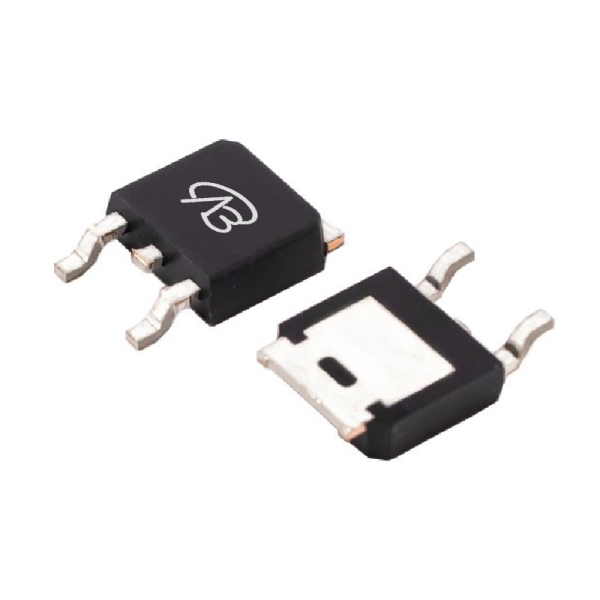
ZXMP7A17KTC-VB is a high-performance unipolar P-type field effect transistor (MOSFET) in TO-252 package, suitable for a variety of power control and switching applications. It has excellent switching characteristics and low on-resistance, can provide efficient current conduction capability, and is suitable for circuit designs requiring higher power handling and low switching losses.
The maximum drain-source voltage (VDS) of this MOSFET is -60V, it can withstand operation under high voltage conditions, and has a high current carrying capacity, with a maximum drain current (ID) of up to -30A. Its ultra-low on-resistance (RDS(ON)) makes it excel in efficient power conversion and thermal management. The product has a wide gate-source voltage (VGS) control range, up to ±20V, providing flexible options for different control circuits.
File download

Download PDF document
 Download now
Product parameter:
| VB Package | Configuration | VDS(V) | VGS | Vthyp(V) | ID(A) | Rds2.5 | Rds4.5 | Rds10 | Technology |
|---|---|---|---|---|---|---|---|---|---|
| TO252 | Single-P | -60V | -1.7V | -30A | 100mΩ | 90mΩ | Trench |
| VB Package | Configuration | VCE | VGE | VGEth(V) | VCEsat15V | ICE | Technology |
|---|---|---|---|---|---|---|---|
| TO252 | Single-P | Trench |
| VB Package | Configuration | VDS(V) | VGS | Vthyp(V) | ID(A) | Rds18 | Technology |
|---|---|---|---|---|---|---|---|
| TO252 | Single-P | -60V | -1.7V | -30A | Trench |
| VB Package | Configuration | VDS(V) | VGS | Vthyp(V) | ID(A) | Rds6 | Technology |
|---|---|---|---|---|---|---|---|
| TO252 | Single-P | -60V | -1.7V | -30A | Trench |
| VB Package | Polarity | Vz / VR | Pd | VF | IF | IR | Cd | Type |
|---|---|---|---|---|---|---|---|---|
| TO252 | Single-P |
ZXMP7A17KTC-VB parameter description:
| Parameter | Value | Description |
|-----------------|--------------------------|--------------------------|
| **Package** | TO-252 | Three-terminal package, suitable for surface mounting|
| **Configuration** | Single P-type channel | Suitable for load switching and power management|
| **VDS (drain-source voltage)** | -60V | Maximum drain-source voltage is -60V |
| **VGS (gate-source voltage)** | ±20V | Gate-source voltage control range|
| **Vth (gate threshold voltage)** | -1.7V | Gate threshold voltage|
| **RDS(ON)** | 100mΩ @ VGS = 4.5V | On-resistance when gate-source voltage is 4.5V|
| | 90mΩ @ VGS = 10V | Gate-source voltage is 10V |
| **ID (Drain Current)** | -30A | Maximum Drain Current|
| **Technology** | Trench Technology | Provides low on-resistance and fast switching response|
Domain and module applications:
Application areas and module examples of ZXMP7A17KTC-VB:
1. **Power management system**: ZXMP7A17KTC-VB is suitable for power switching circuits, especially in DC-DC converters, due to its low on-resistance and high current carrying capacity. It can be used in efficient power conversion and load regulation modules to improve the energy efficiency of the overall system.
2. **Motor drive module**: In motor drive circuits, especially low voltage or high current application scenarios, ZXMP7A17KTC-VB's high current carrying capacity and excellent switching characteristics make it an ideal choice. It can achieve efficient starting, running and stopping of the motor, reduce power loss and improve thermal management.
3. **Inverter**: In inverters, especially solar inverters and other high power converters, ZXMP7A17KTC-VB provides good switching performance, can efficiently convert DC power to AC power, and work stably under high load conditions to reduce energy loss.
4. **Load Switch Circuit**: Due to its low RDS(ON) and high current capability, this MOSFET is suitable for various load switch circuits, including overcurrent protection, load connection or disconnection control and other scenarios.
5. **Smart Home Appliances**: In some smart home appliances, such as power tools, household appliances, etc., ZXMP7A17KTC-VB can be used as a current control, switch and regulation module to optimize energy efficiency and improve the operating stability of the equipment.
6. **Battery Management System**: ZXMP7A17KTC-VB is used in the battery management system (BMS) to control battery charging and discharging, which can ensure that the battery operates within a safe range and optimize the power loss during charging and discharging.
The low on-resistance and wide gate-source voltage control range of this MOSFET make it an ideal choice for various power management and power switching applications, suitable for circuit designs that require high current, high efficiency and stability.
Technical support:
* If you have any questions about the product, please fill out the form to submit, we will reply you within 24 hours


