 中文
中文 English
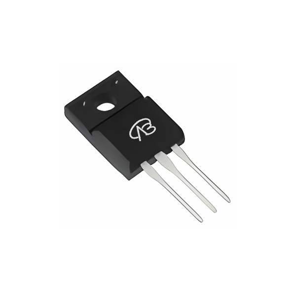
TSM7N60-VB TO220F Product details
 Back to previous page
Product introduction:
1. **Product Introduction - TSM7N60-VB (TO220F)**
TSM7N60-VB is a single N-Channel power MOSFET in TO220F package with extremely high voltage tolerance and a maximum drain-source voltage (V_DS) of 650V. The device adopts Plannar technology and has excellent current switching characteristics, which is particularly suitable for high-voltage power supply control and switching circuits. Its gate drive voltage (V_GS) is ±30V and the gate threshold voltage (V_th) is 3.5V, which is suitable for various high-voltage applications.
The on-resistance (R_DS(ON)) of TSM7N60-VB is 1100mΩ, which shows low power loss at a gate drive voltage of 10V and supports a maximum drain current (I_D) of 7A. The excellent performance of this MOSFET makes it widely used in high-voltage, high-current power management, current switching and high-efficiency converters.
TSM7N60-VB is a single N-Channel power MOSFET in TO220F package with extremely high voltage tolerance and a maximum drain-source voltage (V_DS) of 650V. The device adopts Plannar technology and has excellent current switching characteristics, which is particularly suitable for high-voltage power supply control and switching circuits. Its gate drive voltage (V_GS) is ±30V and the gate threshold voltage (V_th) is 3.5V, which is suitable for various high-voltage applications.
The on-resistance (R_DS(ON)) of TSM7N60-VB is 1100mΩ, which shows low power loss at a gate drive voltage of 10V and supports a maximum drain current (I_D) of 7A. The excellent performance of this MOSFET makes it widely used in high-voltage, high-current power management, current switching and high-efficiency converters.
File download

Download PDF document
 Download now
Product parameter:
| VB Package | Configuration | VDS(V) | VGS | Vthyp(V) | ID(A) | Rds2.5 | Rds4.5 | Rds10 | Technology |
|---|---|---|---|---|---|---|---|---|---|
| TO220F | Single-N | 650V | 3.5V | 7A | 1100mΩ | Plannar |
| VB Package | Configuration | VCE | VGE | VGEth(V) | VCEsat15V | ICE | Technology |
|---|---|---|---|---|---|---|---|
| TO220F | Single-N | Plannar |
| VB Package | Configuration | VDS(V) | VGS | Vthyp(V) | ID(A) | Rds18 | Technology |
|---|---|---|---|---|---|---|---|
| TO220F | Single-N | 650V | 3.5V | 7A | Plannar |
| VB Package | Configuration | VDS(V) | VGS | Vthyp(V) | ID(A) | Rds6 | Technology |
|---|---|---|---|---|---|---|---|
| TO220F | Single-N | 650V | 3.5V | 7A | Plannar |
| VB Package | Polarity | Vz / VR | Pd | VF | IF | IR | Cd | Type |
|---|---|---|---|---|---|---|---|---|
| TO220F | Single-N |
2. **Detailed parameter description**
- **Model**: TSM7N60-VB
- **Package type**: TO220F
- **Configuration**: Single N-Channel
- **Drain to source voltage (V_DS)**: 650V
- **Gate drive voltage (V_GS)**: ±30V
- **Gate threshold voltage (V_th)**: 3.5V
- **On-resistance (R_DS(ON))**:
- 1100mΩ @ V_GS = 10V
- **Maximum drain current (I_D)**: 7A
- **Maximum power dissipation (P_D)**: 75W
- **Maximum junction temperature**: +150°C
- **Technology type**: Plannar
- **Switching characteristics**:
- Turn-on delay time (t_d(on)): 18ns
- Turn-off delay time (t_d(off)): 20ns
- **Maximum gate-source voltage (V_GS_max)**: ±30V
- **Thermal resistance (RthJC)**: 1.7°C/W (typical)
- **Junction temperature range**: -55°C to +150°C
- **Reverse recovery time (T_rr)**: 30ns (typical)
- **Reverse leakage current (I_DSS)**: ≤250nA @ V_DS = 650V
- **Model**: TSM7N60-VB
- **Package type**: TO220F
- **Configuration**: Single N-Channel
- **Drain to source voltage (V_DS)**: 650V
- **Gate drive voltage (V_GS)**: ±30V
- **Gate threshold voltage (V_th)**: 3.5V
- **On-resistance (R_DS(ON))**:
- 1100mΩ @ V_GS = 10V
- **Maximum drain current (I_D)**: 7A
- **Maximum power dissipation (P_D)**: 75W
- **Maximum junction temperature**: +150°C
- **Technology type**: Plannar
- **Switching characteristics**:
- Turn-on delay time (t_d(on)): 18ns
- Turn-off delay time (t_d(off)): 20ns
- **Maximum gate-source voltage (V_GS_max)**: ±30V
- **Thermal resistance (RthJC)**: 1.7°C/W (typical)
- **Junction temperature range**: -55°C to +150°C
- **Reverse recovery time (T_rr)**: 30ns (typical)
- **Reverse leakage current (I_DSS)**: ≤250nA @ V_DS = 650V
Domain and module applications:
3. **Application Fields and Module Examples**
# **High Voltage Power Management Systems**
TSM7N60-VB is widely used in high voltage power management systems, especially for high voltage DC-DC converters, AC-DC power supplies, and uninterruptible power supply (UPS) systems. Its high voltage tolerance of 650V enables it to provide reliable switching control in power conversion and voltage regulation modules with high voltage input.
# **Automotive Electrical Systems**
In automotive electrical systems, TSM7N60-VB can be used for high voltage power and current management systems, especially in high voltage applications such as battery management systems and charging systems for electric vehicles (EV) or hybrid electric vehicles (HEV). Its high voltage tolerance and reliable switching performance enable it to provide efficient power conversion in electric vehicles.
Summary
TSM7N60-VB is an excellent 650V N-Channel MOSFET suitable for a variety of high voltage applications, including power management, current switching, LED drive, motor drive and home appliances. Its high voltage tolerance, low on-resistance and stable switching performance make it an excellent performer in high-efficiency power control systems, especially for high voltage and current-intensive applications.
# **High Voltage Power Management Systems**
TSM7N60-VB is widely used in high voltage power management systems, especially for high voltage DC-DC converters, AC-DC power supplies, and uninterruptible power supply (UPS) systems. Its high voltage tolerance of 650V enables it to provide reliable switching control in power conversion and voltage regulation modules with high voltage input.
# **Automotive Electrical Systems**
In automotive electrical systems, TSM7N60-VB can be used for high voltage power and current management systems, especially in high voltage applications such as battery management systems and charging systems for electric vehicles (EV) or hybrid electric vehicles (HEV). Its high voltage tolerance and reliable switching performance enable it to provide efficient power conversion in electric vehicles.
Summary
TSM7N60-VB is an excellent 650V N-Channel MOSFET suitable for a variety of high voltage applications, including power management, current switching, LED drive, motor drive and home appliances. Its high voltage tolerance, low on-resistance and stable switching performance make it an excellent performer in high-efficiency power control systems, especially for high voltage and current-intensive applications.
* Please note: the above is only an example application scenario, the specific application depends on the requirements and conditions of the system design. When using this device, consult its data sheet for detailed technical specifications and features
Technical support:
* If you have any questions about the product, please fill out the form to submit, we will reply you within 24 hours


