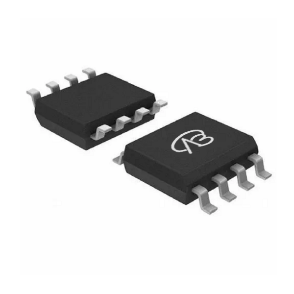
Product parameter:
| VB Package |
Configuration |
VDS(V) |
VGS |
Vthyp(V) |
ID(A) |
Rds2.5 |
Rds4.5 |
Rds10 |
Technology |
| SOP8 |
Dual-N+P |
±30V |
|
1.8/-1.7V |
10/-8A |
|
|
11/21mΩ |
Trench |
| VB Package |
Configuration |
VCE |
VGE |
VGEth(V) |
VCEsat15V |
ICE |
Technology |
| SOP8 |
Dual-N+P |
|
|
|
|
|
Trench |
| VB Package |
Configuration |
VDS(V) |
VGS |
Vthyp(V) |
ID(A) |
Rds18 |
Technology |
| SOP8 |
Dual-N+P |
±30V |
|
1.8/-1.7V |
10/-8A |
|
Trench |
| VB Package |
Configuration |
VDS(V) |
VGS |
Vthyp(V) |
ID(A) |
Rds6 |
Technology |
| SOP8 |
Dual-N+P |
±30V |
|
1.8/-1.7V |
10/-8A |
|
Trench |
| VB Package |
Polarity |
Vz / VR |
Pd |
VF |
IF |
IR |
Cd |
Type |
| SOP8 |
Dual-N+P |
|
|
|
|
|
|
|
SSG4505-VB MOSFET detailed parameter description
- **Package type**: SOP8
- **Configuration**: Dual-N+P-Channel
- **Maximum drain-source voltage (VDS)**: ±30V
- **Maximum gate-source voltage (VGS)**: ±20V
- **Threshold voltage (Vth)**:
- N channel: 1.8V
- P channel: -1.7V
- **On-resistance (RDS(ON))**:
- N channel: 13mΩ @ VGS = 4.5V, 11mΩ @ VGS = 10V
- P channel: 28mΩ @ VGS = 4.5V, 21mΩ @ VGS = 10V
- **Maximum drain current (ID)**:
- N channel: 10A
- P channel: -8A
- **Maximum power dissipation**: 80W (based on temperature conditions)
- **Operating temperature range**: -55°C to +150°C
- **Technology**: Trench
- **Quiet leakage current**: Very low quiescent leakage current to ensure low power loss
- **Switching characteristics**: Fast switching response, suitable for high frequency applications
---
Domain and module applications:
SSG4505-VB MOSFET Application Fields and Module Examples
1. **Power Management System**
SSG4505-VB can be used as a positive and negative polarity switching element in a power management system to perform efficient current switching in a bipolar power system. Its dual N+P channel configuration is suitable for applications such as DC-DC converters, battery management systems, and uninterruptible power supplies (UPS). Its low on-resistance and efficient switching performance make it an ideal choice for power conversion modules.
2. **Load Switch**
Due to its bipolar switching characteristics, SSG4505-VB can be used in load switch modules, especially in applications where positive and negative power control is required. For example, in the fields of LED driving, power tools, and battery-powered systems, this MOSFET can be used to efficiently control the on and off of the load, reduce power loss, and improve system efficiency.
3. **Battery Protection and Management**
SSG4505-VB is widely used in battery protection and management systems. Its combination of N-channel and P-channel enables it to provide bipolar current control, which is suitable for efficient battery charge and discharge management and overcurrent protection. In the battery management system of electric vehicles (EV) and mobile devices, SSG4505-VB can be used to switch battery circuits to ensure safe and stable battery working conditions.
4. **Communication power system**
In the communication power system, SSG4505-VB can be used in power converters and voltage regulator circuits. It can efficiently handle bidirectional currents and is suitable for power modules in communication equipment, including base station power supplies, data center power supplies, and power management of other wireless communication equipment.
5. **Power conversion and inverter applications**
SSG4505-VB is suitable for small power converters and inverters, especially those that need to manage positive and negative power at the same time. Its low RDS(ON) and high switching performance are suitable for use in power converters, inverters, motor drives and other power conditioning systems, and can provide efficient current control and reduce energy losses.
6. **Low-power applications**
In low-power systems, the low on-resistance and low static leakage current of SSG4505-VB make it suitable for various low-power power and switching applications. For example, portable devices, battery-powered devices and other occasions require efficient energy conversion and control, and SSG4505-VB provides ideal performance through efficient switching and low power loss.
7. **DC-DC converter**
In various DC-DC converter applications, SSG4505-VB, as a switching element, can effectively manage input and output currents and provide efficient voltage conversion. Its dual N+P channel configuration can simplify circuit design and improve conversion efficiency. It is suitable for various small and medium-power DC-DC conversion modules, such as adapters, vehicle power supplies and wireless device power modules.
8. **Automotive electronics**
Due to its voltage resistance and bipolar switching characteristics, SSG4505-VB is also suitable for power control modules in automotive electronic systems. It can be used in the battery management system, power control system and on-board power module of electric vehicles to achieve efficient power management and control, and improve the stability and efficiency of the automotive electrical system.
---
SSG4505-VB MOSFET is widely used in power management, battery protection, load switching, power tools, battery drive and small power converters through its dual N+P channel design, high switching performance, low on-resistance and high current handling capability. These features make it excellent in a variety of high-efficiency, low-power loss applications.
* Please note: the above is only an example application scenario, the specific application depends on the requirements and conditions of the system design. When using this device, consult its data sheet for detailed technical specifications and features


 Download now

 中文
中文 English
 Back to previous page