 中文
中文 English
SI6926EDQ-T1-E3-VB Product details
 Back to previous page
Product introduction:
Product Introduction:
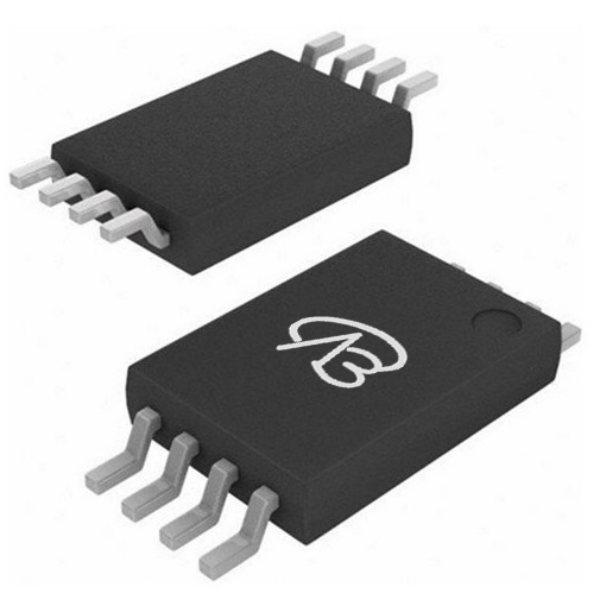
**SI6926EDQ-T1-E3-VB** is a dual N-channel power MOSFET in **TSSOP8 package**, configured as **Common Drain** N+N-Channel** structure, designed for low voltage and high efficiency applications. The maximum drain-source voltage (V_DS) of this MOSFET is 20V, the gate-source voltage (V_GS) is ±20V, and the switching threshold voltage (V_th) is between 0.5V and 1.5V. Its on-resistance (R_DS(ON)) is 32mΩ at V_GS = 2.5V and 22mΩ at V_GS = 4.5V, with low conduction loss and high-efficiency switching characteristics. The maximum drain current (I_D) is 6.6A, enabling it to meet the needs of low- and medium-power power management and switching power supplies. Using **Trench** technology, SI6926EDQ-T1-E3-VB provides excellent thermal stability and reliability, suitable for various applications with high requirements on power efficiency.
**SI6926EDQ-T1-E3-VB** is a dual N-channel power MOSFET in **TSSOP8 package**, configured as **Common Drain** N+N-Channel** structure, designed for low voltage and high efficiency applications. The maximum drain-source voltage (V_DS) of this MOSFET is 20V, the gate-source voltage (V_GS) is ±20V, and the switching threshold voltage (V_th) is between 0.5V and 1.5V. Its on-resistance (R_DS(ON)) is 32mΩ at V_GS = 2.5V and 22mΩ at V_GS = 4.5V, with low conduction loss and high-efficiency switching characteristics. The maximum drain current (I_D) is 6.6A, enabling it to meet the needs of low- and medium-power power management and switching power supplies. Using **Trench** technology, SI6926EDQ-T1-E3-VB provides excellent thermal stability and reliability, suitable for various applications with high requirements on power efficiency.
File download

Download PDF document
 Download now
Product parameter:
| VB Package | Configuration | VDS(V) | VGS | Vthyp(V) | ID(A) | Rds2.5 | Rds4.5 | Rds10 | Technology |
|---|---|---|---|---|---|---|---|---|---|
| TSSOP8 | Common Drain-N+N | 20V | 0.5~1.5V | 6.6A | 32mΩ | Trench |
| VB Package | Configuration | VCE | VGE | VGEth(V) | VCEsat15V | ICE | Technology |
|---|---|---|---|---|---|---|---|
| TSSOP8 | Common Drain-N+N | Trench |
| VB Package | Configuration | VDS(V) | VGS | Vthyp(V) | ID(A) | Rds18 | Technology |
|---|---|---|---|---|---|---|---|
| TSSOP8 | Common Drain-N+N | 20V | 0.5~1.5V | 6.6A | Trench |
| VB Package | Configuration | VDS(V) | VGS | Vthyp(V) | ID(A) | Rds6 | Technology |
|---|---|---|---|---|---|---|---|
| TSSOP8 | Common Drain-N+N | 20V | 0.5~1.5V | 6.6A | Trench |
| VB Package | Polarity | Vz / VR | Pd | VF | IF | IR | Cd | Type |
|---|---|---|---|---|---|---|---|---|
| TSSOP8 | Common Drain-N+N |
Detailed parameter description:
- **Model**: SI6926EDQ-T1-E3-VB
- **Package**: TSSOP8
- **Configuration**: Common Drain N+N-Channel
- **Maximum drain-source voltage (V_DS)**: 20V
- **Gate-source voltage (V_GS)**: ±20V
- **Switching threshold voltage (V_th)**: 0.5V ~ 1.5V
- **On-resistance (R_DS(ON))**:
- 32mΩ @ V_GS = 2.5V
- 22mΩ @ V_GS = 4.5V
- **Maximum drain current (I_D)**: 6.6A
- **Technology**: Trench technology
- **Maximum Power Dissipation (P_D)**: 100W (depending on heat dissipation conditions)
- **Reverse Recovery Time**: Typical fast switching performance, suitable for high frequency switching applications
- **Operating Temperature Range**: -55°C to +150°C
- **Gate Charge (Qg)**: 16nC (V_GS = 4.5V)
- **Pin Configuration**: Standard TSSOP8 package, suitable for compact designs
- **Model**: SI6926EDQ-T1-E3-VB
- **Package**: TSSOP8
- **Configuration**: Common Drain N+N-Channel
- **Maximum drain-source voltage (V_DS)**: 20V
- **Gate-source voltage (V_GS)**: ±20V
- **Switching threshold voltage (V_th)**: 0.5V ~ 1.5V
- **On-resistance (R_DS(ON))**:
- 32mΩ @ V_GS = 2.5V
- 22mΩ @ V_GS = 4.5V
- **Maximum drain current (I_D)**: 6.6A
- **Technology**: Trench technology
- **Maximum Power Dissipation (P_D)**: 100W (depending on heat dissipation conditions)
- **Reverse Recovery Time**: Typical fast switching performance, suitable for high frequency switching applications
- **Operating Temperature Range**: -55°C to +150°C
- **Gate Charge (Qg)**: 16nC (V_GS = 4.5V)
- **Pin Configuration**: Standard TSSOP8 package, suitable for compact designs
Domain and module applications:
Application fields and module examples:
1. **DC-DC converter**:
**SI6926EDQ-T1-E3-VB** is used as the main switching element in the DC-DC converter and is widely used in scenarios where low voltage input is efficiently converted. Its low on-resistance (R_DS(ON)) can significantly reduce energy loss during the conversion process and improve overall system efficiency. It is suitable for a variety of battery-powered devices such as laptops, portable power supplies, and smart home devices.
2. **Battery Management System (BMS)**:
In the battery management system, **SI6926EDQ-T1-E3-VB** is used as a switching control element to efficiently control the battery charging and discharging process to ensure the safety and long life of the battery. The high efficiency and low on-resistance characteristics of this MOSFET make it particularly suitable for applications in battery charging management, power tools, electric bicycles, and other battery-driven systems.
3. **Power Adapter and Charger**:
In power adapter and charger modules, **SI6926EDQ-T1-E3-VB** can be used as a high-frequency switching element to optimize power conversion efficiency. It can effectively reduce heat loss and is suitable for modules such as chargers, battery managers and portable power supplies, especially in portable devices that require efficient power conversion.
4. **LED Driver**:
**SI6926EDQ-T1-E3-VB**'s fast switching performance and low on-resistance make it very suitable for use in LED driver power supplies, which can reduce power consumption while ensuring stable current output. This MOSFET can be used in efficient LED lighting systems, suitable for residential, commercial and automotive lighting and other fields, ensuring long-term stable operation of LEDs.
5. **Load Switch and Current Control**:
As a dual N-channel MOSFET in a common source configuration, **SI6926EDQ-T1-E3-VB** is very suitable for load switch control. Whether it is used for current control or load switching applications, the low on-resistance and high current capability make it perform well in load current regulation. It is suitable for use in various home appliances, consumer electronics, and industrial equipment for fast switching and precise current control.
6. **High-efficiency switching power supply (SMPS)**:
**SI6926EDQ-T1-E3-VB**'s high switching speed and low on-resistance make it very cost-effective in high-efficiency switching power supply (SMPS) applications. This MOSFET can maintain low power loss at high frequency and is suitable for a variety of power conversion applications such as power conversion, boost, and buck. It is particularly suitable for power management modules in data centers, communication equipment, and consumer electronics.
7. **Automotive electronic systems**:
In automotive electronic systems, **SI6926EDQ-T1-E3-VB** can be used as power management and load switching components, especially in applications such as battery charging management, electric vehicle (EV) charging piles, and on-board chargers. This MOSFET can effectively improve power conversion efficiency, reduce system energy loss, and ensure efficient operation of automotive electronic systems.
1. **DC-DC converter**:
**SI6926EDQ-T1-E3-VB** is used as the main switching element in the DC-DC converter and is widely used in scenarios where low voltage input is efficiently converted. Its low on-resistance (R_DS(ON)) can significantly reduce energy loss during the conversion process and improve overall system efficiency. It is suitable for a variety of battery-powered devices such as laptops, portable power supplies, and smart home devices.
2. **Battery Management System (BMS)**:
In the battery management system, **SI6926EDQ-T1-E3-VB** is used as a switching control element to efficiently control the battery charging and discharging process to ensure the safety and long life of the battery. The high efficiency and low on-resistance characteristics of this MOSFET make it particularly suitable for applications in battery charging management, power tools, electric bicycles, and other battery-driven systems.
3. **Power Adapter and Charger**:
In power adapter and charger modules, **SI6926EDQ-T1-E3-VB** can be used as a high-frequency switching element to optimize power conversion efficiency. It can effectively reduce heat loss and is suitable for modules such as chargers, battery managers and portable power supplies, especially in portable devices that require efficient power conversion.
4. **LED Driver**:
**SI6926EDQ-T1-E3-VB**'s fast switching performance and low on-resistance make it very suitable for use in LED driver power supplies, which can reduce power consumption while ensuring stable current output. This MOSFET can be used in efficient LED lighting systems, suitable for residential, commercial and automotive lighting and other fields, ensuring long-term stable operation of LEDs.
5. **Load Switch and Current Control**:
As a dual N-channel MOSFET in a common source configuration, **SI6926EDQ-T1-E3-VB** is very suitable for load switch control. Whether it is used for current control or load switching applications, the low on-resistance and high current capability make it perform well in load current regulation. It is suitable for use in various home appliances, consumer electronics, and industrial equipment for fast switching and precise current control.
6. **High-efficiency switching power supply (SMPS)**:
**SI6926EDQ-T1-E3-VB**'s high switching speed and low on-resistance make it very cost-effective in high-efficiency switching power supply (SMPS) applications. This MOSFET can maintain low power loss at high frequency and is suitable for a variety of power conversion applications such as power conversion, boost, and buck. It is particularly suitable for power management modules in data centers, communication equipment, and consumer electronics.
7. **Automotive electronic systems**:
In automotive electronic systems, **SI6926EDQ-T1-E3-VB** can be used as power management and load switching components, especially in applications such as battery charging management, electric vehicle (EV) charging piles, and on-board chargers. This MOSFET can effectively improve power conversion efficiency, reduce system energy loss, and ensure efficient operation of automotive electronic systems.
* Please note: the above is only an example application scenario, the specific application depends on the requirements and conditions of the system design. When using this device, consult its data sheet for detailed technical specifications and features
Technical support:
* If you have any questions about the product, please fill out the form to submit, we will reply you within 24 hours


