 中文
中文 English
NCE01P30K-VB Product details
 Back to previous page
Product introduction:
NCE01P30K-VB Product Introduction
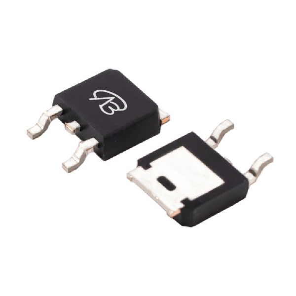
NCE01P30K-VB is a high-performance unipolar P-type MOSFET in a **TO252** package, suitable for applications requiring high voltage and high current control. The device has a drain-source voltage (VDS) of **-100V** and a gate-source voltage (VGS) of **±20V**. Its on-resistance (RDS(ON)) is **37mΩ** at VGS = 4.5V and **33mΩ** at VGS = 10V, respectively, ensuring low conduction losses and improving system efficiency. Due to its **Trench technology** providing excellent switching performance and low on-resistance, the device is widely used in power management systems that require high reliability and high energy efficiency. The maximum drain current of this MOSFET is **-40A**, suitable for a variety of power conversion and high power control fields.
---
NCE01P30K-VB is a high-performance unipolar P-type MOSFET in a **TO252** package, suitable for applications requiring high voltage and high current control. The device has a drain-source voltage (VDS) of **-100V** and a gate-source voltage (VGS) of **±20V**. Its on-resistance (RDS(ON)) is **37mΩ** at VGS = 4.5V and **33mΩ** at VGS = 10V, respectively, ensuring low conduction losses and improving system efficiency. Due to its **Trench technology** providing excellent switching performance and low on-resistance, the device is widely used in power management systems that require high reliability and high energy efficiency. The maximum drain current of this MOSFET is **-40A**, suitable for a variety of power conversion and high power control fields.
---
File download

Download PDF document
 Download now
Product parameter:
| VB Package | Configuration | VDS(V) | VGS | Vthyp(V) | ID(A) | Rds2.5 | Rds4.5 | Rds10 | Technology |
|---|---|---|---|---|---|---|---|---|---|
| TO252 | Single-P | -100V | -2V | -40A | 33mΩ | Trench |
| VB Package | Configuration | VCE | VGE | VGEth(V) | VCEsat15V | ICE | Technology |
|---|---|---|---|---|---|---|---|
| TO252 | Single-P | Trench |
| VB Package | Configuration | VDS(V) | VGS | Vthyp(V) | ID(A) | Rds18 | Technology |
|---|---|---|---|---|---|---|---|
| TO252 | Single-P | -100V | -2V | -40A | Trench |
| VB Package | Configuration | VDS(V) | VGS | Vthyp(V) | ID(A) | Rds6 | Technology |
|---|---|---|---|---|---|---|---|
| TO252 | Single-P | -100V | -2V | -40A | Trench |
| VB Package | Polarity | Vz / VR | Pd | VF | IF | IR | Cd | Type |
|---|---|---|---|---|---|---|---|---|
| TO252 | Single-P |
Detailed parameter description
| **Parameter** | **Value** |
|--------------------------|-------------------------|
| **Model** | NCE01P30K-VB |
| **Package** | TO252 |
| **Configuration** | Unipolar P-type|
| **Maximum drain-source voltage (VDS)** | -100V |
| **Maximum gate-source voltage (VGS)** | ±20V |
| **Threshold voltage (Vth)** | -2V |
| **On-resistance (RDS(ON))** | 37mΩ @ VGS = 4.5V |
| | 33mΩ @ VGS = 10V |
| **Maximum drain current (ID)** | -40A |
| **Technology** | Trench |
---
| **Parameter** | **Value** |
|--------------------------|-------------------------|
| **Model** | NCE01P30K-VB |
| **Package** | TO252 |
| **Configuration** | Unipolar P-type|
| **Maximum drain-source voltage (VDS)** | -100V |
| **Maximum gate-source voltage (VGS)** | ±20V |
| **Threshold voltage (Vth)** | -2V |
| **On-resistance (RDS(ON))** | 37mΩ @ VGS = 4.5V |
| | 33mΩ @ VGS = 10V |
| **Maximum drain current (ID)** | -40A |
| **Technology** | Trench |
---
Domain and module applications:
Application fields and modules
1. **Load switch and reverse current protection**
NCE01P30K-VB can be used as a load switch to provide stable high current control in scenarios where efficient load switching is required. At the same time, it is suitable for use in reverse current protection circuits to help prevent reverse current in the power system from damaging sensitive devices.
2. **Battery Management System (BMS)**
In lithium battery protection and charge and discharge control, P-type MOSFET is one of the key components. NCE01P30K-VB can provide reliable high voltage control to ensure safe and efficient operation of batteries, and is widely used in electric vehicles and energy storage systems.
3. **DC motor control**
In the motor reversal control circuit, this P-type MOSFET makes motor control more precise and reduces power consumption through low on-resistance and high current handling capability, and is suitable for home appliances, industrial control equipment and robotics.
4. **Solar Inverter and Power Management**
NCE01P30K-VB is suitable for high-efficiency control modules of solar power conversion systems. With its good conduction performance and current capability, it improves the overall conversion efficiency and reliability of the system.
5. **Automotive Electronics System**
This device can be used in automotive power management modules to control load power supply and voltage protection, providing high-efficiency solutions for the power systems of modern electric vehicles and hybrid vehicles.
With its excellent switching performance and power control capabilities, NCE01P30K-VB has demonstrated excellent application value in multiple high-demand fields, ensuring high reliability and energy efficiency optimization of system operation.
1. **Load switch and reverse current protection**
NCE01P30K-VB can be used as a load switch to provide stable high current control in scenarios where efficient load switching is required. At the same time, it is suitable for use in reverse current protection circuits to help prevent reverse current in the power system from damaging sensitive devices.
2. **Battery Management System (BMS)**
In lithium battery protection and charge and discharge control, P-type MOSFET is one of the key components. NCE01P30K-VB can provide reliable high voltage control to ensure safe and efficient operation of batteries, and is widely used in electric vehicles and energy storage systems.
3. **DC motor control**
In the motor reversal control circuit, this P-type MOSFET makes motor control more precise and reduces power consumption through low on-resistance and high current handling capability, and is suitable for home appliances, industrial control equipment and robotics.
4. **Solar Inverter and Power Management**
NCE01P30K-VB is suitable for high-efficiency control modules of solar power conversion systems. With its good conduction performance and current capability, it improves the overall conversion efficiency and reliability of the system.
5. **Automotive Electronics System**
This device can be used in automotive power management modules to control load power supply and voltage protection, providing high-efficiency solutions for the power systems of modern electric vehicles and hybrid vehicles.
With its excellent switching performance and power control capabilities, NCE01P30K-VB has demonstrated excellent application value in multiple high-demand fields, ensuring high reliability and energy efficiency optimization of system operation.
* Please note: the above is only an example application scenario, the specific application depends on the requirements and conditions of the system design. When using this device, consult its data sheet for detailed technical specifications and features
Technical support:
* If you have any questions about the product, please fill out the form to submit, we will reply you within 24 hours


