 中文
中文 English
ME10N03-VB Product details
 Back to previous page
Product introduction:
1. ME10N03-VB Product Introduction
ME10N03-VB is a **single N-channel MOSFET** in **TO252** package, with **30V drain-source voltage (VDS)** and ±20V gate drive voltage (VGS). The **turn-on voltage Vth of the device is 1.7V**, and its on-resistance shows excellent performance under different gate voltage conditions:
- **9mΩ** @ VGS = 4.5V
- **7mΩ** @ VGS = 10V
ME10N03-VB supports **maximum 70A continuous drain current (ID)**, and is manufactured using **trench technology**, with low conduction loss and excellent switching performance, suitable for high-frequency and high-efficiency power conversion applications.
---
ME10N03-VB is a **single N-channel MOSFET** in **TO252** package, with **30V drain-source voltage (VDS)** and ±20V gate drive voltage (VGS). The **turn-on voltage Vth of the device is 1.7V**, and its on-resistance shows excellent performance under different gate voltage conditions:
- **9mΩ** @ VGS = 4.5V
- **7mΩ** @ VGS = 10V
ME10N03-VB supports **maximum 70A continuous drain current (ID)**, and is manufactured using **trench technology**, with low conduction loss and excellent switching performance, suitable for high-frequency and high-efficiency power conversion applications.
---
File download

Download PDF document
 Download now
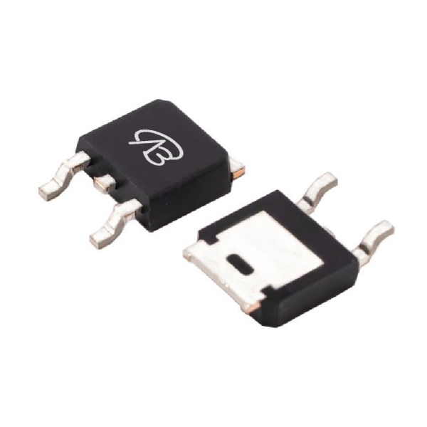
Product parameter:
| VB Package | Configuration | VDS(V) | VGS | Vthyp(V) | ID(A) | Rds2.5 | Rds4.5 | Rds10 | Technology |
|---|---|---|---|---|---|---|---|---|---|
| TO252 | Single-N | 30V | 1.7V | 70A | 7mΩ | Trench |
| VB Package | Configuration | VCE | VGE | VGEth(V) | VCEsat15V | ICE | Technology |
|---|---|---|---|---|---|---|---|
| TO252 | Single-N | Trench |
| VB Package | Configuration | VDS(V) | VGS | Vthyp(V) | ID(A) | Rds18 | Technology |
|---|---|---|---|---|---|---|---|
| TO252 | Single-N | 30V | 1.7V | 70A | Trench |
| VB Package | Configuration | VDS(V) | VGS | Vthyp(V) | ID(A) | Rds6 | Technology |
|---|---|---|---|---|---|---|---|
| TO252 | Single-N | 30V | 1.7V | 70A | Trench |
| VB Package | Polarity | Vz / VR | Pd | VF | IF | IR | Cd | Type |
|---|---|---|---|---|---|---|---|---|
| TO252 | Single-N |
2. ME10N03-VB Detailed Parameter Description
| **Parameter** | **Value** | **Description** |
|------------------|------------------------------|----------------------------------------------|
| **Package Type** | TO252 | Surface mount package, suitable for high power and high current applications|
| **MOSFET Configuration** | Single N-channel | Single N-type channel, suitable for high-speed switching applications|
| **Drain-Source Voltage (VDS)** | 30V | Maximum drain-source voltage, suitable for low-voltage power supply system|
| **Gate Voltage (VGS)** | ±20V | Gate drive voltage range, improve application flexibility|
| **Turning Voltage (Vth)** | 1.7V | Turn-on threshold voltage of MOSFET|
| **On-resistance (RDS(ON))** | 9mΩ @ VGS = 4.5V
7mΩ @ VGS = 10V | Low on-resistance, reduced power consumption, improved efficiency|
| **Maximum drain current (ID)**| 70A | Supports high current load applications|
| **Technology** | Trench | Trench technology reduces conduction loss and switching loss|
---
| **Parameter** | **Value** | **Description** |
|------------------|------------------------------|----------------------------------------------|
| **Package Type** | TO252 | Surface mount package, suitable for high power and high current applications|
| **MOSFET Configuration** | Single N-channel | Single N-type channel, suitable for high-speed switching applications|
| **Drain-Source Voltage (VDS)** | 30V | Maximum drain-source voltage, suitable for low-voltage power supply system|
| **Gate Voltage (VGS)** | ±20V | Gate drive voltage range, improve application flexibility|
| **Turning Voltage (Vth)** | 1.7V | Turn-on threshold voltage of MOSFET|
| **On-resistance (RDS(ON))** | 9mΩ @ VGS = 4.5V
7mΩ @ VGS = 10V | Low on-resistance, reduced power consumption, improved efficiency|
| **Maximum drain current (ID)**| 70A | Supports high current load applications|
| **Technology** | Trench | Trench technology reduces conduction loss and switching loss|
---
Domain and module applications:
III. Application fields and module examples
1. **Power management and DC-DC converters**
- ME10N03-VB is suitable for various **DC-DC converters** and power management modules, especially in portable devices, consumer electronics and computer power supplies, where its low on-resistance and high current capability can significantly improve system efficiency.
2. **Motor drive and control**
- This MOSFET is suitable for **motor drive modules**, such as DC motor control in power tools and home appliances. Due to its fast switching capability and high current handling capability, efficient motor control can be achieved.
3. **LED drive circuits**
- ME10N03-VB can also be applied to **LED drive circuits** as a switching element in lighting systems and displays to ensure stable current output and improve energy efficiency.
4. **Battery Management System (BMS)**
- In **Battery Management System**, this MOSFET can be used as a protection switch for the battery, which can efficiently control the charging and discharging process to ensure safety and stability.
5. **Smart Home Devices**
- This device is widely used in **Smart Home** systems, such as automatically controlled sockets, switches and dimmers, providing low power consumption and efficient power switching functions.
As a high-performance MOSFET, ME10N03-VB is an ideal choice for modern power management and control circuits with its excellent electrical characteristics and wide range of applications.
1. **Power management and DC-DC converters**
- ME10N03-VB is suitable for various **DC-DC converters** and power management modules, especially in portable devices, consumer electronics and computer power supplies, where its low on-resistance and high current capability can significantly improve system efficiency.
2. **Motor drive and control**
- This MOSFET is suitable for **motor drive modules**, such as DC motor control in power tools and home appliances. Due to its fast switching capability and high current handling capability, efficient motor control can be achieved.
3. **LED drive circuits**
- ME10N03-VB can also be applied to **LED drive circuits** as a switching element in lighting systems and displays to ensure stable current output and improve energy efficiency.
4. **Battery Management System (BMS)**
- In **Battery Management System**, this MOSFET can be used as a protection switch for the battery, which can efficiently control the charging and discharging process to ensure safety and stability.
5. **Smart Home Devices**
- This device is widely used in **Smart Home** systems, such as automatically controlled sockets, switches and dimmers, providing low power consumption and efficient power switching functions.
As a high-performance MOSFET, ME10N03-VB is an ideal choice for modern power management and control circuits with its excellent electrical characteristics and wide range of applications.
* Please note: the above is only an example application scenario, the specific application depends on the requirements and conditions of the system design. When using this device, consult its data sheet for detailed technical specifications and features
Technical support:
* If you have any questions about the product, please fill out the form to submit, we will reply you within 24 hours


