 中文
中文 English
L3402S-VB Product details
 Back to previous page
Product introduction:
1. Product Introduction of L3402S-VB MOSFET
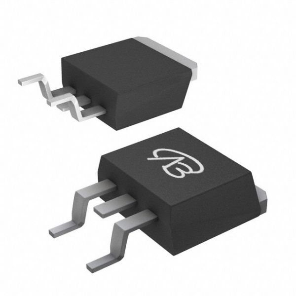
L3402S-VB is a high-efficiency single N-channel MOSFET designed with TO263 package, optimized for low voltage and high current applications. The device has a drain-source voltage (VDS) of 20V, a gate-source voltage (VGS) of ±20V, and a wide turn-on threshold voltage (Vth) range of 0.5V to 1.5V. This enables the L3402S-VB to operate efficiently under a variety of control conditions. Its on-resistance (RDS(ON)) performs well, at 9mΩ at VGS of 2.5V and 6mΩ at 4.5V, and the maximum drain current (ID) can reach 85A. L3402S-VB uses advanced trench technology, which can provide excellent thermal performance and high efficiency, and is very suitable for high-power applications in multiple fields.
L3402S-VB is a high-efficiency single N-channel MOSFET designed with TO263 package, optimized for low voltage and high current applications. The device has a drain-source voltage (VDS) of 20V, a gate-source voltage (VGS) of ±20V, and a wide turn-on threshold voltage (Vth) range of 0.5V to 1.5V. This enables the L3402S-VB to operate efficiently under a variety of control conditions. Its on-resistance (RDS(ON)) performs well, at 9mΩ at VGS of 2.5V and 6mΩ at 4.5V, and the maximum drain current (ID) can reach 85A. L3402S-VB uses advanced trench technology, which can provide excellent thermal performance and high efficiency, and is very suitable for high-power applications in multiple fields.
File download

Download PDF document
 Download now
Product parameter:
| VB Package | Configuration | VDS(V) | VGS | Vthyp(V) | ID(A) | Rds2.5 | Rds4.5 | Rds10 | Technology |
|---|---|---|---|---|---|---|---|---|---|
| TO263 | Single-N | 20V | 0.5~1.5V | 85A | 9mΩ | Trench |
| VB Package | Configuration | VCE | VGE | VGEth(V) | VCEsat15V | ICE | Technology |
|---|---|---|---|---|---|---|---|
| TO263 | Single-N | Trench |
| VB Package | Configuration | VDS(V) | VGS | Vthyp(V) | ID(A) | Rds18 | Technology |
|---|---|---|---|---|---|---|---|
| TO263 | Single-N | 20V | 0.5~1.5V | 85A | Trench |
| VB Package | Configuration | VDS(V) | VGS | Vthyp(V) | ID(A) | Rds6 | Technology |
|---|---|---|---|---|---|---|---|
| TO263 | Single-N | 20V | 0.5~1.5V | 85A | Trench |
| VB Package | Polarity | Vz / VR | Pd | VF | IF | IR | Cd | Type |
|---|---|---|---|---|---|---|---|---|
| TO263 | Single-N |
2. Detailed parameter description of L3402S-VB MOSFET
- **Package type**: TO263
- **Polarity configuration**: Single N-channel
- **Drain-source voltage (VDS)**: 20V
- **Gate-source voltage (VGS)**: ±20V
- **Turning threshold voltage (Vth)**: 0.5V to 1.5V
- **On-resistance (RDS(ON))**:
- 9mΩ@VGS=2.5V
- 6mΩ@VGS=4.5V
- **Maximum drain current (ID)**: 85A
- **Technology**: Trench technology
- **Power dissipation**: The maximum power dissipation capability depends on the heat dissipation conditions, usually around 100W. The specific value needs to refer to the thermal characteristics table.
- **Operating temperature range**: -55°C to 150°C, please refer to detailed technical documents for specific values.
- **Number of package pins**: 3 pins
- **Package type**: TO263
- **Polarity configuration**: Single N-channel
- **Drain-source voltage (VDS)**: 20V
- **Gate-source voltage (VGS)**: ±20V
- **Turning threshold voltage (Vth)**: 0.5V to 1.5V
- **On-resistance (RDS(ON))**:
- 9mΩ@VGS=2.5V
- 6mΩ@VGS=4.5V
- **Maximum drain current (ID)**: 85A
- **Technology**: Trench technology
- **Power dissipation**: The maximum power dissipation capability depends on the heat dissipation conditions, usually around 100W. The specific value needs to refer to the thermal characteristics table.
- **Operating temperature range**: -55°C to 150°C, please refer to detailed technical documents for specific values.
- **Number of package pins**: 3 pins
Domain and module applications:
3. Application fields and applicable module examples of L3402S-VB MOSFET
1. **Power management**
L3402S-VB is suitable for efficient power management systems, including switching power supplies (SMPS) and DC-DC converters. Its low on-resistance can significantly reduce power consumption and heat, improve the overall efficiency of the system, and is widely used in consumer electronics and industrial power supply equipment.
2. **Motor drive**
In motor control applications, the high current carrying capacity of L3402S-VB makes it very suitable for driving DC motors and stepper motors. It can provide stable current during motor startup and operation, and is used in automation equipment, robots and power tools.
3. **LED drive**
L3402S-VB is very suitable for use in LED lighting systems, and can effectively control the operating current of LEDs to ensure efficient operation of LEDs. Due to its excellent conduction characteristics, the device performs well in applications such as LED lamps and backlight modules, improving the overall lighting effect.
4. **Battery Management System**
This MOSFET is also suitable for battery management systems (BMS), providing efficient switch control during charging and discharging to ensure battery stability and safety. Its application in electric vehicles and renewable energy systems is increasing, helping to achieve higher energy utilization.
In general, the L3402S-VB MOSFET is suitable for multiple high-efficiency applications with its excellent current handling capability and low power consumption characteristics, meeting the high power and efficiency requirements of modern electronic products.
1. **Power management**
L3402S-VB is suitable for efficient power management systems, including switching power supplies (SMPS) and DC-DC converters. Its low on-resistance can significantly reduce power consumption and heat, improve the overall efficiency of the system, and is widely used in consumer electronics and industrial power supply equipment.
2. **Motor drive**
In motor control applications, the high current carrying capacity of L3402S-VB makes it very suitable for driving DC motors and stepper motors. It can provide stable current during motor startup and operation, and is used in automation equipment, robots and power tools.
3. **LED drive**
L3402S-VB is very suitable for use in LED lighting systems, and can effectively control the operating current of LEDs to ensure efficient operation of LEDs. Due to its excellent conduction characteristics, the device performs well in applications such as LED lamps and backlight modules, improving the overall lighting effect.
4. **Battery Management System**
This MOSFET is also suitable for battery management systems (BMS), providing efficient switch control during charging and discharging to ensure battery stability and safety. Its application in electric vehicles and renewable energy systems is increasing, helping to achieve higher energy utilization.
In general, the L3402S-VB MOSFET is suitable for multiple high-efficiency applications with its excellent current handling capability and low power consumption characteristics, meeting the high power and efficiency requirements of modern electronic products.
* Please note: the above is only an example application scenario, the specific application depends on the requirements and conditions of the system design. When using this device, consult its data sheet for detailed technical specifications and features
Technical support:
* If you have any questions about the product, please fill out the form to submit, we will reply you within 24 hours


