 中文
中文 English
JCS50N06RH-VB Product details
 Back to previous page
Product introduction:
JCS50N06RH-VB MOSFET Product Introduction
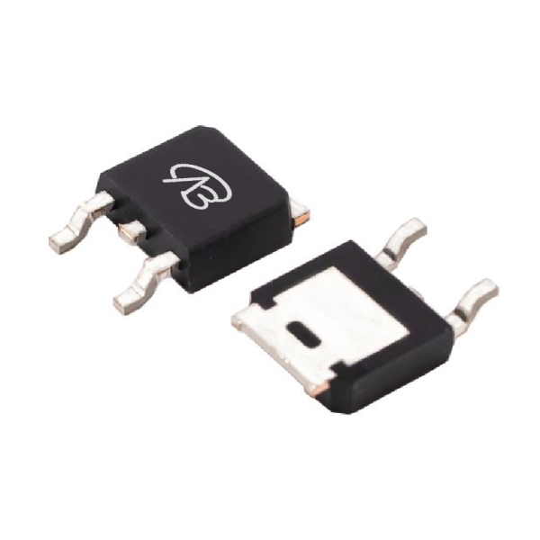
**JCS50N06RH-VB** is a high-performance N-type MOSFET in TO-252 package, designed for medium and high voltage applications. The maximum drain-source voltage (VDS) of the device is 60V, suitable for various power management and switching circuits. The maximum gate-source voltage (VGS) is ±20V, ensuring stable operation of the device under safe conditions. The on-resistance (RDS(ON)) of JCS50N06RH-VB is 13mΩ at VGS=4.5V and 10mΩ at VGS=10V, providing excellent low power consumption performance. Using Trench technology, this MOSFET can still maintain good operating stability at high temperatures, which is very suitable for modern power electronics applications.
---
**JCS50N06RH-VB** is a high-performance N-type MOSFET in TO-252 package, designed for medium and high voltage applications. The maximum drain-source voltage (VDS) of the device is 60V, suitable for various power management and switching circuits. The maximum gate-source voltage (VGS) is ±20V, ensuring stable operation of the device under safe conditions. The on-resistance (RDS(ON)) of JCS50N06RH-VB is 13mΩ at VGS=4.5V and 10mΩ at VGS=10V, providing excellent low power consumption performance. Using Trench technology, this MOSFET can still maintain good operating stability at high temperatures, which is very suitable for modern power electronics applications.
---
File download

Download PDF document
 Download now
Product parameter:
| VB Package | Configuration | VDS(V) | VGS | Vthyp(V) | ID(A) | Rds2.5 | Rds4.5 | Rds10 | Technology |
|---|---|---|---|---|---|---|---|---|---|
| TO252 | Single-N | 60V | 2.5V | 58A | 10mΩ | Trench |
| VB Package | Configuration | VCE | VGE | VGEth(V) | VCEsat15V | ICE | Technology |
|---|---|---|---|---|---|---|---|
| TO252 | Single-N | Trench |
| VB Package | Configuration | VDS(V) | VGS | Vthyp(V) | ID(A) | Rds18 | Technology |
|---|---|---|---|---|---|---|---|
| TO252 | Single-N | 60V | 2.5V | 58A | Trench |
| VB Package | Configuration | VDS(V) | VGS | Vthyp(V) | ID(A) | Rds6 | Technology |
|---|---|---|---|---|---|---|---|
| TO252 | Single-N | 60V | 2.5V | 58A | Trench |
| VB Package | Polarity | Vz / VR | Pd | VF | IF | IR | Cd | Type |
|---|---|---|---|---|---|---|---|---|
| TO252 | Single-N |
Detailed parameter description
1. **Package**: TO-252
- TO-252 package design provides good heat dissipation performance, suitable for medium to high power applications.
2. **Configuration**: Single N-type channel
- Single channel configuration allows effective control of current, suitable for a variety of circuit designs.
3. **Drain-source voltage (VDS)**: 60V
- The maximum drain-source voltage that the device can withstand, suitable for medium voltage circuit applications.
4. **Gate-source voltage (VGS)**: ±20V
- The maximum allowable voltage between the gate and source, ensuring the safety and stability of the device.
5. **Threshold voltage (Vth)**: 2.5V
- The minimum gate voltage required for the device to start conducting, providing good switching characteristics.
6. **On-resistance (RDS(ON))**:
- 13mΩ @ VGS = 4.5V
- 10mΩ @ VGS = 10V
- Low on-resistance enables high efficiency and low heat generation during operation.
7. **Current Rating (ID)**: 58A
- The maximum continuous current that the device can handle under normal operating conditions, suitable for high load applications.
8. **Technology**: Trench
- Trench technology provides excellent switching characteristics and low conduction losses, suitable for high-efficiency power electronics design.
---
1. **Package**: TO-252
- TO-252 package design provides good heat dissipation performance, suitable for medium to high power applications.
2. **Configuration**: Single N-type channel
- Single channel configuration allows effective control of current, suitable for a variety of circuit designs.
3. **Drain-source voltage (VDS)**: 60V
- The maximum drain-source voltage that the device can withstand, suitable for medium voltage circuit applications.
4. **Gate-source voltage (VGS)**: ±20V
- The maximum allowable voltage between the gate and source, ensuring the safety and stability of the device.
5. **Threshold voltage (Vth)**: 2.5V
- The minimum gate voltage required for the device to start conducting, providing good switching characteristics.
6. **On-resistance (RDS(ON))**:
- 13mΩ @ VGS = 4.5V
- 10mΩ @ VGS = 10V
- Low on-resistance enables high efficiency and low heat generation during operation.
7. **Current Rating (ID)**: 58A
- The maximum continuous current that the device can handle under normal operating conditions, suitable for high load applications.
8. **Technology**: Trench
- Trench technology provides excellent switching characteristics and low conduction losses, suitable for high-efficiency power electronics design.
---
Domain and module applications:
Application Examples
1. **Power Supply**:
JCS50N06RH-VB is very suitable for high-efficiency power converters and switching power supplies, which can effectively reduce power consumption and improve energy conversion efficiency.
2. **Power Tools**:
This MOSFET can be used in the motor drive control of power tools to ensure stable current and power during startup and operation.
3. **Electric Vehicle**:
In the drive system of electric vehicles, JCS50N06RH-VB can be used for battery management and motor drive to improve overall energy efficiency and performance.
4. **LED Lighting**:
This device is also suitable for LED lighting drive circuits. Its low on-resistance characteristics can effectively improve the brightness and stability of LEDs.
In summary, JCS50N06RH-VB is an N-type MOSFET suitable for a variety of medium and high voltage power electronic applications. It has become an important part of modern electronic design due to its high efficiency, low power consumption and stability.
1. **Power Supply**:
JCS50N06RH-VB is very suitable for high-efficiency power converters and switching power supplies, which can effectively reduce power consumption and improve energy conversion efficiency.
2. **Power Tools**:
This MOSFET can be used in the motor drive control of power tools to ensure stable current and power during startup and operation.
3. **Electric Vehicle**:
In the drive system of electric vehicles, JCS50N06RH-VB can be used for battery management and motor drive to improve overall energy efficiency and performance.
4. **LED Lighting**:
This device is also suitable for LED lighting drive circuits. Its low on-resistance characteristics can effectively improve the brightness and stability of LEDs.
In summary, JCS50N06RH-VB is an N-type MOSFET suitable for a variety of medium and high voltage power electronic applications. It has become an important part of modern electronic design due to its high efficiency, low power consumption and stability.
* Please note: the above is only an example application scenario, the specific application depends on the requirements and conditions of the system design. When using this device, consult its data sheet for detailed technical specifications and features
Technical support:
* If you have any questions about the product, please fill out the form to submit, we will reply you within 24 hours


