 中文
中文 English
JCS10N60FT-O-F-N-B-VB Product details
 Back to previous page
Product introduction:
JCS10N60FT-OFNB-VB MOSFET Product Introduction
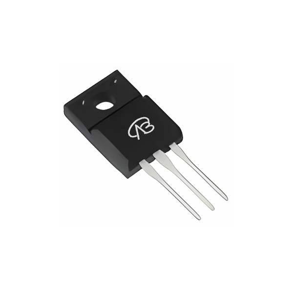
JCS10N60FT-OFNB-VB is a high voltage N-channel MOSFET in TO220F package, designed for high power applications. Its drain-source voltage (VDS) is up to 650V, and the gate-source voltage (VGS) is rated at ±30V, which is suitable for various industrial and power electronics applications. The threshold voltage (Vth) of this MOSFET is 3.5V, and the on-resistance (RDS(ON)) is 680mΩ at VGS=10V, which can effectively reduce the conduction loss. In addition, its maximum drain current (ID) can reach 12A, which meets the needs of high power loads. The planar technology (Plannar) of JCS10N60FT-OFNB-VB ensures its stability and reliability, making it an ideal choice for various harsh environments.
JCS10N60FT-OFNB-VB is a high voltage N-channel MOSFET in TO220F package, designed for high power applications. Its drain-source voltage (VDS) is up to 650V, and the gate-source voltage (VGS) is rated at ±30V, which is suitable for various industrial and power electronics applications. The threshold voltage (Vth) of this MOSFET is 3.5V, and the on-resistance (RDS(ON)) is 680mΩ at VGS=10V, which can effectively reduce the conduction loss. In addition, its maximum drain current (ID) can reach 12A, which meets the needs of high power loads. The planar technology (Plannar) of JCS10N60FT-OFNB-VB ensures its stability and reliability, making it an ideal choice for various harsh environments.
File download

Download PDF document
 Download now
Product parameter:
| VB Package | Configuration | VDS(V) | VGS | Vthyp(V) | ID(A) | Rds2.5 | Rds4.5 | Rds10 | Technology |
|---|---|---|---|---|---|---|---|---|---|
| TO220F | Single-N | 650V | 3.5V | 12A | 680mΩ | Plannar |
| VB Package | Configuration | VCE | VGE | VGEth(V) | VCEsat15V | ICE | Technology |
|---|---|---|---|---|---|---|---|
| TO220F | Single-N | Plannar |
| VB Package | Configuration | VDS(V) | VGS | Vthyp(V) | ID(A) | Rds18 | Technology |
|---|---|---|---|---|---|---|---|
| TO220F | Single-N | 650V | 3.5V | 12A | Plannar |
| VB Package | Configuration | VDS(V) | VGS | Vthyp(V) | ID(A) | Rds6 | Technology |
|---|---|---|---|---|---|---|---|
| TO220F | Single-N | 650V | 3.5V | 12A | Plannar |
| VB Package | Polarity | Vz / VR | Pd | VF | IF | IR | Cd | Type |
|---|---|---|---|---|---|---|---|---|
| TO220F | Single-N |
Detailed parameter description
- **Package**: TO220F
- **Configuration**: Single N-channel
- **VDS (drain-source voltage)**: 650V
- **VGS (gate-source voltage)**: ±30V
- **Vth (threshold voltage)**: 3.5V
- **RDS(ON) (on-resistance)**:
- 680mΩ @ VGS = 10V
- **ID (drain current)**: 12A
- **Technology**: Planar technology
- **Power dissipation (Pd)**: Can handle higher power and has good thermal management capabilities
- **Operating temperature range**: -55°C to 150°C (Tj max)
- **Gate charge (Qg)**: Provides low gate charge characteristics to ensure efficient switching performance.
- **Package**: TO220F
- **Configuration**: Single N-channel
- **VDS (drain-source voltage)**: 650V
- **VGS (gate-source voltage)**: ±30V
- **Vth (threshold voltage)**: 3.5V
- **RDS(ON) (on-resistance)**:
- 680mΩ @ VGS = 10V
- **ID (drain current)**: 12A
- **Technology**: Planar technology
- **Power dissipation (Pd)**: Can handle higher power and has good thermal management capabilities
- **Operating temperature range**: -55°C to 150°C (Tj max)
- **Gate charge (Qg)**: Provides low gate charge characteristics to ensure efficient switching performance.
Domain and module applications:
Applications and modules
JCS10N60FT-OFNB-VB MOSFET has a wide range of applications in multiple fields, mainly including:
1. **Power management**: Due to its high voltage capability and low on-resistance, JCS10N60FT-OFNB-VB MOSFET is very suitable for high-voltage DC-DC converters and switching power supplies. Its application in power electronic equipment can significantly improve energy efficiency and reduce power consumption.
2. **Motor drive**: This MOSFET can be widely used in motor control, such as motor drive systems for home appliances, power tools and electric vehicles. The leakage current capability of up to 12A enables it to meet the driving needs of high-power motors, especially in high-voltage and high-power applications.
3. **Lighting control**: JCS10N60FT-OFNB-VB MOSFET can be used for LED driving and lamp control. Its high voltage characteristics and fast switching capability make it a key component in smart lighting solutions.
4. **Power Switch**: This MOSFET is suitable for various switching applications, including power switching and load switching, and can efficiently control high-power loads. This is widely used in industrial equipment, communication equipment, and automotive electronics.
The high performance and reliability of the JCS10N60FT-OFNB-VB MOSFET make it an ideal choice in various power electronics applications.
JCS10N60FT-OFNB-VB MOSFET has a wide range of applications in multiple fields, mainly including:
1. **Power management**: Due to its high voltage capability and low on-resistance, JCS10N60FT-OFNB-VB MOSFET is very suitable for high-voltage DC-DC converters and switching power supplies. Its application in power electronic equipment can significantly improve energy efficiency and reduce power consumption.
2. **Motor drive**: This MOSFET can be widely used in motor control, such as motor drive systems for home appliances, power tools and electric vehicles. The leakage current capability of up to 12A enables it to meet the driving needs of high-power motors, especially in high-voltage and high-power applications.
3. **Lighting control**: JCS10N60FT-OFNB-VB MOSFET can be used for LED driving and lamp control. Its high voltage characteristics and fast switching capability make it a key component in smart lighting solutions.
4. **Power Switch**: This MOSFET is suitable for various switching applications, including power switching and load switching, and can efficiently control high-power loads. This is widely used in industrial equipment, communication equipment, and automotive electronics.
The high performance and reliability of the JCS10N60FT-OFNB-VB MOSFET make it an ideal choice in various power electronics applications.
* Please note: the above is only an example application scenario, the specific application depends on the requirements and conditions of the system design. When using this device, consult its data sheet for detailed technical specifications and features
Technical support:
* If you have any questions about the product, please fill out the form to submit, we will reply you within 24 hours


