 中文
中文 English
J651-VB Product details
 Back to previous page
Product introduction:
1. J651-VB Product Introduction
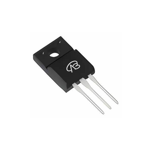
J651-VB is a high-performance P-channel MOSFET in TO220F package, designed for high current and high voltage applications. Its drain-source voltage (VDS) can reach -60V and the maximum drain current (ID) is -30A, which is suitable for various power electronic devices. With a threshold voltage (Vth) of -1.7V, the device has excellent switching performance and can operate efficiently at low voltage. With its low on-resistance of 60mΩ (@VGS=4.5V) and 50mΩ (@VGS=10V), J651-VB provides excellent energy efficiency and is suitable for a wide range of power management and control systems.
J651-VB is a high-performance P-channel MOSFET in TO220F package, designed for high current and high voltage applications. Its drain-source voltage (VDS) can reach -60V and the maximum drain current (ID) is -30A, which is suitable for various power electronic devices. With a threshold voltage (Vth) of -1.7V, the device has excellent switching performance and can operate efficiently at low voltage. With its low on-resistance of 60mΩ (@VGS=4.5V) and 50mΩ (@VGS=10V), J651-VB provides excellent energy efficiency and is suitable for a wide range of power management and control systems.
File download

Download PDF document
 Download now
Product parameter:
| VB Package | Configuration | VDS(V) | VGS | Vthyp(V) | ID(A) | Rds2.5 | Rds4.5 | Rds10 | Technology |
|---|---|---|---|---|---|---|---|---|---|
| TO220F | Single-P | -60V | -1.7V | -30A | 50mΩ | Trench |
| VB Package | Configuration | VCE | VGE | VGEth(V) | VCEsat15V | ICE | Technology |
|---|---|---|---|---|---|---|---|
| TO220F | Single-P | Trench |
| VB Package | Configuration | VDS(V) | VGS | Vthyp(V) | ID(A) | Rds18 | Technology |
|---|---|---|---|---|---|---|---|
| TO220F | Single-P | -60V | -1.7V | -30A | Trench |
| VB Package | Configuration | VDS(V) | VGS | Vthyp(V) | ID(A) | Rds6 | Technology |
|---|---|---|---|---|---|---|---|
| TO220F | Single-P | -60V | -1.7V | -30A | Trench |
| VB Package | Polarity | Vz / VR | Pd | VF | IF | IR | Cd | Type |
|---|---|---|---|---|---|---|---|---|
| TO220F | Single-P |
2. Detailed parameter description of J651-VB
- **Model**: J651-VB
- **Package type**: TO220F
- **Configuration**: Single P-channel
- **Drain-source voltage (VDS)**: -60V
- **Gate-source voltage (VGS)**: ±20V
- **Threshold voltage (Vth)**: -1.7V
- **On-resistance (RDS(ON))**:
- 60mΩ (@VGS=4.5V)
- 50mΩ (@VGS=10V)
- **Maximum drain current (ID)**: -30A
- **Technology**: Trench
- **Operating temperature range**: -55°C to 175°C
- **Power consumption**: The specific power consumption varies according to the actual application circuit
- **Switching speed**: Suitable for fast switching applications
- **Voltage resistance**: High voltage resistance, suitable for high voltage circuit design
- **Model**: J651-VB
- **Package type**: TO220F
- **Configuration**: Single P-channel
- **Drain-source voltage (VDS)**: -60V
- **Gate-source voltage (VGS)**: ±20V
- **Threshold voltage (Vth)**: -1.7V
- **On-resistance (RDS(ON))**:
- 60mΩ (@VGS=4.5V)
- 50mΩ (@VGS=10V)
- **Maximum drain current (ID)**: -30A
- **Technology**: Trench
- **Operating temperature range**: -55°C to 175°C
- **Power consumption**: The specific power consumption varies according to the actual application circuit
- **Switching speed**: Suitable for fast switching applications
- **Voltage resistance**: High voltage resistance, suitable for high voltage circuit design
Domain and module applications:
III. Application fields and module examples of J651-VB
1. **Power management and power conversion modules**
J651-VB performs well in power management systems and is often used in DC-DC converters and AC-DC power modules. Its low on-resistance helps improve energy efficiency and reduce heat loss, and is widely used in uninterruptible power supplies (UPS) and computer power supplies to achieve efficient power conversion and management.
2. **Motor drive and control**
The device is suitable for high-efficiency motor drive applications, such as motor control circuits in electric vehicles and automation equipment. The load capacity and fast switching characteristics of J651-VB can effectively control the starting and speed regulation of the motor, thereby improving the efficiency and performance of the entire system.
3. **Load switch and protection circuit**
J651-VB can also be used as a switch for high-current loads, and is often used in battery management systems (BMS) and intelligent power distribution systems to ensure the safety and reliability of the circuit. By monitoring the current load, the device can effectively protect the equipment from overcurrent or short circuit, extending the service life of the equipment.
4. **Renewable Energy Systems**
J651-VB also has superior performance in power management modules for solar inverters and wind power generation. It can handle rapidly changing currents, provide efficient energy conversion and storage solutions for renewable energy systems, and meet the strict requirements of modern energy systems for efficiency and reliability.
In general, J651-VB is an efficient and reliable MOSFET suitable for a variety of power electronics applications, providing excellent performance and reliability for modern power supply designs.
1. **Power management and power conversion modules**
J651-VB performs well in power management systems and is often used in DC-DC converters and AC-DC power modules. Its low on-resistance helps improve energy efficiency and reduce heat loss, and is widely used in uninterruptible power supplies (UPS) and computer power supplies to achieve efficient power conversion and management.
2. **Motor drive and control**
The device is suitable for high-efficiency motor drive applications, such as motor control circuits in electric vehicles and automation equipment. The load capacity and fast switching characteristics of J651-VB can effectively control the starting and speed regulation of the motor, thereby improving the efficiency and performance of the entire system.
3. **Load switch and protection circuit**
J651-VB can also be used as a switch for high-current loads, and is often used in battery management systems (BMS) and intelligent power distribution systems to ensure the safety and reliability of the circuit. By monitoring the current load, the device can effectively protect the equipment from overcurrent or short circuit, extending the service life of the equipment.
4. **Renewable Energy Systems**
J651-VB also has superior performance in power management modules for solar inverters and wind power generation. It can handle rapidly changing currents, provide efficient energy conversion and storage solutions for renewable energy systems, and meet the strict requirements of modern energy systems for efficiency and reliability.
In general, J651-VB is an efficient and reliable MOSFET suitable for a variety of power electronics applications, providing excellent performance and reliability for modern power supply designs.
* Please note: the above is only an example application scenario, the specific application depends on the requirements and conditions of the system design. When using this device, consult its data sheet for detailed technical specifications and features
Technical support:
* If you have any questions about the product, please fill out the form to submit, we will reply you within 24 hours


