 中文
中文 English
HM1N60R-VB Product details
 Back to previous page
Product introduction:
1. HM1N60R-VB Product Introduction
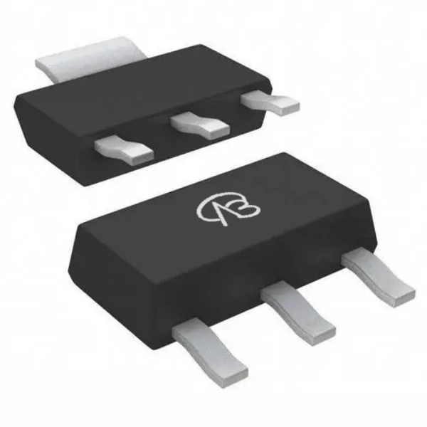
HM1N60R-VB is a high-voltage single N-channel MOSFET in a SOT223 package, designed for high voltage and low current applications. The MOSFET has a drain-source voltage (VDS) of 650V, making it suitable for operation in high voltage environments. Its gate-source voltage (VGS) is a maximum of ±30V, and its threshold voltage (Vth) is 3.5V, enabling stable switching at relatively low gate voltages. The on-resistance (RDS(ON)) of the HM1N60R-VB is 8000mΩ at VGS=10V and 10000mΩ at VGS=4.5V, and the relatively high on-resistance makes it suitable for low current applications. The device supports a continuous drain current (ID) of up to 1A and uses Plannar technology, which is suitable for applications that require high voltage tolerance but low current requirements.
HM1N60R-VB is a high-voltage single N-channel MOSFET in a SOT223 package, designed for high voltage and low current applications. The MOSFET has a drain-source voltage (VDS) of 650V, making it suitable for operation in high voltage environments. Its gate-source voltage (VGS) is a maximum of ±30V, and its threshold voltage (Vth) is 3.5V, enabling stable switching at relatively low gate voltages. The on-resistance (RDS(ON)) of the HM1N60R-VB is 8000mΩ at VGS=10V and 10000mΩ at VGS=4.5V, and the relatively high on-resistance makes it suitable for low current applications. The device supports a continuous drain current (ID) of up to 1A and uses Plannar technology, which is suitable for applications that require high voltage tolerance but low current requirements.
File download

Download PDF document
 Download now
Product parameter:
| VB Package | Configuration | VDS(V) | VGS | Vthyp(V) | ID(A) | Rds2.5 | Rds4.5 | Rds10 | Technology |
|---|---|---|---|---|---|---|---|---|---|
| SOT223 | Single-N | 650V | 3.5V | 1A | 8000mΩ | Plannar |
| VB Package | Configuration | VCE | VGE | VGEth(V) | VCEsat15V | ICE | Technology |
|---|---|---|---|---|---|---|---|
| SOT223 | Single-N | Plannar |
| VB Package | Configuration | VDS(V) | VGS | Vthyp(V) | ID(A) | Rds18 | Technology |
|---|---|---|---|---|---|---|---|
| SOT223 | Single-N | 650V | 3.5V | 1A | Plannar |
| VB Package | Configuration | VDS(V) | VGS | Vthyp(V) | ID(A) | Rds6 | Technology |
|---|---|---|---|---|---|---|---|
| SOT223 | Single-N | 650V | 3.5V | 1A | Plannar |
| VB Package | Polarity | Vz / VR | Pd | VF | IF | IR | Cd | Type |
|---|---|---|---|---|---|---|---|---|
| SOT223 | Single-N |
II. Detailed parameter description of HM1N60R-VB
1. **Package type**: SOT223
2. **Channel configuration**: Single N-channel
3. **Drain-source voltage (VDS)**: 650V
4. **Gate-source voltage (VGS)**: ±30V
5. **Threshold voltage (Vth)**: 3.5V
6. **On-resistance (RDS(ON))**:
- 8000mΩ @ VGS=10V
- 10000mΩ @ VGS=4.5V
7. **Continuous drain current (ID)**: 1A
8. **Technology type**: Plannar
9. **Breakdown voltage (BVDSS)**: 650V
10. **Maximum power dissipation (Ptot)**: 1.25W
11. **Operating temperature range**: -55°C to +150°C
12. **Input capacitance (Ciss)**: 700pF
13. **Output capacitance (Coss)**: 100pF
14. **Reverse recovery time (trr)**: 200ns
1. **Package type**: SOT223
2. **Channel configuration**: Single N-channel
3. **Drain-source voltage (VDS)**: 650V
4. **Gate-source voltage (VGS)**: ±30V
5. **Threshold voltage (Vth)**: 3.5V
6. **On-resistance (RDS(ON))**:
- 8000mΩ @ VGS=10V
- 10000mΩ @ VGS=4.5V
7. **Continuous drain current (ID)**: 1A
8. **Technology type**: Plannar
9. **Breakdown voltage (BVDSS)**: 650V
10. **Maximum power dissipation (Ptot)**: 1.25W
11. **Operating temperature range**: -55°C to +150°C
12. **Input capacitance (Ciss)**: 700pF
13. **Output capacitance (Coss)**: 100pF
14. **Reverse recovery time (trr)**: 200ns
Domain and module applications:
3. Application fields and modules of HM1N60R-VB
The high voltage tolerance and moderate current handling capability of HM1N60R-VB MOSFET make it very effective in some specific application fields. Here are some typical application fields and modules:
1. **High voltage switching circuit**: In high voltage power switching and protection circuits, HM1N60R-VB can handle voltages up to 650V, which is very suitable for high voltage switching and fuse functions to ensure the safety and stability of the power system.
2. **Power converter**: This MOSFET is suitable for switching control of high voltage power converters, can operate stably under high voltage conditions, and is suitable for designing power converters that require high voltage isolation, such as AC-DC converters.
3. **Battery protection circuit**: In high voltage battery protection circuits, HM1N60R-VB can provide effective switching functions and protection to ensure the safety of batteries in high voltage operations.
4. **Inverter Application**: This MOSFET is suitable for high-voltage inverters. It can handle high voltage input and provide stable output, which is suitable for photovoltaic inverters and other high-voltage inverter applications.
5. **High-voltage Test Equipment**: HM1N60R-VB can also be used for switching and control in high-voltage test equipment to ensure stability and reliability when testing high-voltage components.
These characteristics make HM1N60R-VB MOSFET have significant advantages in high-voltage applications, providing a reliable solution for various power electronic equipment.
The high voltage tolerance and moderate current handling capability of HM1N60R-VB MOSFET make it very effective in some specific application fields. Here are some typical application fields and modules:
1. **High voltage switching circuit**: In high voltage power switching and protection circuits, HM1N60R-VB can handle voltages up to 650V, which is very suitable for high voltage switching and fuse functions to ensure the safety and stability of the power system.
2. **Power converter**: This MOSFET is suitable for switching control of high voltage power converters, can operate stably under high voltage conditions, and is suitable for designing power converters that require high voltage isolation, such as AC-DC converters.
3. **Battery protection circuit**: In high voltage battery protection circuits, HM1N60R-VB can provide effective switching functions and protection to ensure the safety of batteries in high voltage operations.
4. **Inverter Application**: This MOSFET is suitable for high-voltage inverters. It can handle high voltage input and provide stable output, which is suitable for photovoltaic inverters and other high-voltage inverter applications.
5. **High-voltage Test Equipment**: HM1N60R-VB can also be used for switching and control in high-voltage test equipment to ensure stability and reliability when testing high-voltage components.
These characteristics make HM1N60R-VB MOSFET have significant advantages in high-voltage applications, providing a reliable solution for various power electronic equipment.
* Please note: the above is only an example application scenario, the specific application depends on the requirements and conditions of the system design. When using this device, consult its data sheet for detailed technical specifications and features
Technical support:
* If you have any questions about the product, please fill out the form to submit, we will reply you within 24 hours


