 中文
中文 English
H6968CTS-VB Product details
 Back to previous page
Product introduction:
H6968CTS-VB MOSFET Product Introduction
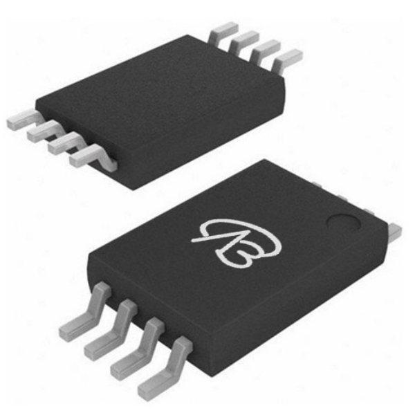
H6968CTS-VB is a common drain dual N-channel MOSFET in TSSOP8 package, based on Trench technology. This MOSFET is designed for low voltage and high efficiency applications, with a drain-source voltage (VDS) of 20V and a maximum drain current (ID) of 7.6A. Its on-resistance is only 14mΩ at VGS=4.5V, which enables it to provide excellent conduction performance at low voltage and is suitable for circuit designs requiring low conduction losses.
H6968CTS-VB is a common drain dual N-channel MOSFET in TSSOP8 package, based on Trench technology. This MOSFET is designed for low voltage and high efficiency applications, with a drain-source voltage (VDS) of 20V and a maximum drain current (ID) of 7.6A. Its on-resistance is only 14mΩ at VGS=4.5V, which enables it to provide excellent conduction performance at low voltage and is suitable for circuit designs requiring low conduction losses.
File download

Download PDF document
 Download now
Product parameter:
| VB Package | Configuration | VDS(V) | VGS | Vthyp(V) | ID(A) | Rds2.5 | Rds4.5 | Rds10 | Technology |
|---|---|---|---|---|---|---|---|---|---|
| TSSOP8 | Common Drain-N+N | 20V | 0.5~1.5V | 7.6A | 18mΩ | Trench |
| VB Package | Configuration | VCE | VGE | VGEth(V) | VCEsat15V | ICE | Technology |
|---|---|---|---|---|---|---|---|
| TSSOP8 | Common Drain-N+N | Trench |
| VB Package | Configuration | VDS(V) | VGS | Vthyp(V) | ID(A) | Rds18 | Technology |
|---|---|---|---|---|---|---|---|
| TSSOP8 | Common Drain-N+N | 20V | 0.5~1.5V | 7.6A | Trench |
| VB Package | Configuration | VDS(V) | VGS | Vthyp(V) | ID(A) | Rds6 | Technology |
|---|---|---|---|---|---|---|---|
| TSSOP8 | Common Drain-N+N | 20V | 0.5~1.5V | 7.6A | Trench |
| VB Package | Polarity | Vz / VR | Pd | VF | IF | IR | Cd | Type |
|---|---|---|---|---|---|---|---|---|
| TSSOP8 | Common Drain-N+N |
H6968CTS-VB MOSFET Detailed parameter description
- **Package**: TSSOP8
- **Channel configuration**: Common drain dual N-channel
- **Drain-source voltage (VDS)**: 20V
- **Gate-source voltage (VGS)**: ±12V
- **Threshold voltage (Vth)**: 0.5V to 1.5V
- **On-resistance (RDS(ON))**:
- 18mΩ @ VGS = 2.5V
- 14mΩ @ VGS = 4.5V
- **Maximum drain current (ID)**: 7.6A
- **Technology type**: Trench technology
- **Package**: TSSOP8
- **Channel configuration**: Common drain dual N-channel
- **Drain-source voltage (VDS)**: 20V
- **Gate-source voltage (VGS)**: ±12V
- **Threshold voltage (Vth)**: 0.5V to 1.5V
- **On-resistance (RDS(ON))**:
- 18mΩ @ VGS = 2.5V
- 14mΩ @ VGS = 4.5V
- **Maximum drain current (ID)**: 7.6A
- **Technology type**: Trench technology
Domain and module applications:
Application fields and modules of H6968CTS-VB MOSFET
The low voltage and high efficiency characteristics of H6968CTS-VB MOSFET make it suitable for the following application fields and modules:
1. **Portable device power management**: This MOSFET is suitable for power management modules in smartphones, tablets and wearable devices. Its low on-resistance and dual N-channel configuration can optimize power consumption in the circuit and extend the battery life of the device. It is suitable for battery protection circuits and low-dropout regulators (LDO).
2. **DC-DC converter**: H6968CTS-VB performs well in DC-DC converters, especially in buck or boost converters that require high efficiency and low conduction losses. Its low on-resistance characteristics can reduce power loss during the conversion process and improve overall efficiency.
3. **Load switch applications**: In low-voltage load switch applications, this MOSFET can provide fast response and efficient switching performance, suitable for small motor control, LED drive circuits and other modules that require high-frequency switching.
4. **Power distribution network (PDN)**: In applications such as servers, routers and storage devices that require high power efficiency, H6968CTS-VB can be used for power switches in power distribution networks to ensure stable power supply and low power consumption.
5. **Consumer electronics**: This MOSFET is widely used in home appliances and other consumer electronics. It can meet the needs of low-voltage operation and provide excellent conduction performance and efficiency. It is suitable for power control and signal conditioning modules.
In summary, H6968CTS-VB is a high-efficiency, low-voltage dual N-channel MOSFET suitable for portable device power management, DC-DC converters, load switches, power distribution networks and consumer electronics. It provides efficient and reliable solutions for these applications.
The low voltage and high efficiency characteristics of H6968CTS-VB MOSFET make it suitable for the following application fields and modules:
1. **Portable device power management**: This MOSFET is suitable for power management modules in smartphones, tablets and wearable devices. Its low on-resistance and dual N-channel configuration can optimize power consumption in the circuit and extend the battery life of the device. It is suitable for battery protection circuits and low-dropout regulators (LDO).
2. **DC-DC converter**: H6968CTS-VB performs well in DC-DC converters, especially in buck or boost converters that require high efficiency and low conduction losses. Its low on-resistance characteristics can reduce power loss during the conversion process and improve overall efficiency.
3. **Load switch applications**: In low-voltage load switch applications, this MOSFET can provide fast response and efficient switching performance, suitable for small motor control, LED drive circuits and other modules that require high-frequency switching.
4. **Power distribution network (PDN)**: In applications such as servers, routers and storage devices that require high power efficiency, H6968CTS-VB can be used for power switches in power distribution networks to ensure stable power supply and low power consumption.
5. **Consumer electronics**: This MOSFET is widely used in home appliances and other consumer electronics. It can meet the needs of low-voltage operation and provide excellent conduction performance and efficiency. It is suitable for power control and signal conditioning modules.
In summary, H6968CTS-VB is a high-efficiency, low-voltage dual N-channel MOSFET suitable for portable device power management, DC-DC converters, load switches, power distribution networks and consumer electronics. It provides efficient and reliable solutions for these applications.
* Please note: the above is only an example application scenario, the specific application depends on the requirements and conditions of the system design. When using this device, consult its data sheet for detailed technical specifications and features
Technical support:
* If you have any questions about the product, please fill out the form to submit, we will reply you within 24 hours


