 中文
中文 English
FQD8P10TM-VB Product details
 Back to previous page
Product introduction:
FQD8P10TM-VB MOSFET Product Introduction
FQD8P10TM-VB is a high-performance P-channel MOSFET in a TO-252 package designed for negative voltage switching and control applications. This MOSFET has a drain-source voltage (VDS) of -100V, suitable for negative voltage environments. Its gate-source voltage (VGS) is ±20V, providing a wide control voltage range. The threshold voltage (Vth) is -2V, ensuring stable conduction at moderate gate voltages. FQD8P10TM-VB uses Trench technology and has a low on-resistance of 280mΩ (at 4.5V gate voltage) and 250mΩ (at 10V gate voltage), respectively. It can carry a continuous drain current (ID) of up to -8.8A, which is very suitable for switching applications with high current loads.
FQD8P10TM-VB is a high-performance P-channel MOSFET in a TO-252 package designed for negative voltage switching and control applications. This MOSFET has a drain-source voltage (VDS) of -100V, suitable for negative voltage environments. Its gate-source voltage (VGS) is ±20V, providing a wide control voltage range. The threshold voltage (Vth) is -2V, ensuring stable conduction at moderate gate voltages. FQD8P10TM-VB uses Trench technology and has a low on-resistance of 280mΩ (at 4.5V gate voltage) and 250mΩ (at 10V gate voltage), respectively. It can carry a continuous drain current (ID) of up to -8.8A, which is very suitable for switching applications with high current loads.
File download

Download PDF document
 Download now
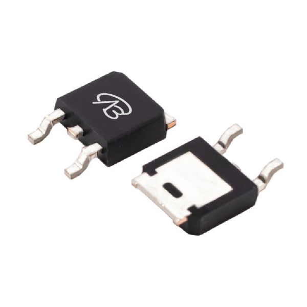
Product parameter:
| VB Package | Configuration | VDS(V) | VGS | Vthyp(V) | ID(A) | Rds2.5 | Rds4.5 | Rds10 | Technology |
|---|---|---|---|---|---|---|---|---|---|
| TO252 | Single-P | -100V | -2V | -8.8A | 250mΩ | Trench |
| VB Package | Configuration | VCE | VGE | VGEth(V) | VCEsat15V | ICE | Technology |
|---|---|---|---|---|---|---|---|
| TO252 | Single-P | Trench |
| VB Package | Configuration | VDS(V) | VGS | Vthyp(V) | ID(A) | Rds18 | Technology |
|---|---|---|---|---|---|---|---|
| TO252 | Single-P | -100V | -2V | -8.8A | Trench |
| VB Package | Configuration | VDS(V) | VGS | Vthyp(V) | ID(A) | Rds6 | Technology |
|---|---|---|---|---|---|---|---|
| TO252 | Single-P | -100V | -2V | -8.8A | Trench |
| VB Package | Polarity | Vz / VR | Pd | VF | IF | IR | Cd | Type |
|---|---|---|---|---|---|---|---|---|
| TO252 | Single-P |
Detailed parameter description of FQD8P10TM-VB
1. **Package**: TO-252
- Surface mount package, suitable for high power applications, providing good heat dissipation and mechanical strength.
2. **Configuration**: Single P channel
- Suitable for high-side switch applications, controlling negative voltage loads, widely used in load control and power management.
3. **Drain-source voltage (VDS)**: -100V
- The maximum drain-to-source voltage allowed, suitable for applications in negative voltage environments.
4. **Gate-source voltage (VGS)**: ±20V
- The maximum voltage allowed to be applied between the gate and the source, providing flexibility for the control circuit.
5. **Threshold voltage (Vth)**: -2V
- The minimum gate voltage required to turn on the MOSFET, suitable for negative voltage control applications.
6. **On-resistance (RDS(ON))**: 280mΩ @ VGS=4.5V; 250mΩ @ VGS=10V
- The drain-to-source resistance of MOSFET at different gate voltages, affecting switching efficiency and power consumption.
7. **Continuous drain current (ID)**: -8.8A
- The maximum current that MOSFET can carry under continuous working conditions, suitable for applications with high current loads.
8. **Technology**: Trench
- Using Trench technology, it provides low on-resistance and high switching efficiency, reduces power consumption and improves system performance.
1. **Package**: TO-252
- Surface mount package, suitable for high power applications, providing good heat dissipation and mechanical strength.
2. **Configuration**: Single P channel
- Suitable for high-side switch applications, controlling negative voltage loads, widely used in load control and power management.
3. **Drain-source voltage (VDS)**: -100V
- The maximum drain-to-source voltage allowed, suitable for applications in negative voltage environments.
4. **Gate-source voltage (VGS)**: ±20V
- The maximum voltage allowed to be applied between the gate and the source, providing flexibility for the control circuit.
5. **Threshold voltage (Vth)**: -2V
- The minimum gate voltage required to turn on the MOSFET, suitable for negative voltage control applications.
6. **On-resistance (RDS(ON))**: 280mΩ @ VGS=4.5V; 250mΩ @ VGS=10V
- The drain-to-source resistance of MOSFET at different gate voltages, affecting switching efficiency and power consumption.
7. **Continuous drain current (ID)**: -8.8A
- The maximum current that MOSFET can carry under continuous working conditions, suitable for applications with high current loads.
8. **Technology**: Trench
- Using Trench technology, it provides low on-resistance and high switching efficiency, reduces power consumption and improves system performance.
Domain and module applications:
Application Examples of FQD8P10TM-VB
FQD8P10TM-VB MOSFET is suitable for a variety of negative voltage and high current switching applications due to its negative voltage tolerance and low on-resistance. Here are some specific application examples:
1. **High-side switch**: In negative voltage power supply systems, FQD8P10TM-VB can be used as a high-side switch to control negative voltage input or output, ensuring efficient and stable operation of the power supply system.
2. **Load switching**: In load switching applications, such as negative voltage load circuit breakers and load protection circuits, FQD8P10TM-VB can reliably control load switching, protect circuits and improve system safety.
3. **Motor drive**: In negative voltage drive circuits that need to control medium current motors, FQD8P10TM-VB can effectively switch current to support the start, run and stop of motors, especially in negative voltage environments.
4. **Industrial control systems**: In industrial automation and control systems, FQD8P10TM-VB is used for load switching and power management to ensure reliable operation of equipment in negative voltage environments.
5. **Power converters**: In DC-DC converters and power conversion modules in negative voltage environments, FQD8P10TM-VB is able to handle negative voltage loads and support switching and current control during voltage conversion.
FQD8P10TM-VB MOSFET, with its negative voltage tolerance and low on-resistance, provides an efficient switching solution for negative voltage and high current applications. Its Trench technology further improves switching efficiency and is suitable for a variety of power and control application scenarios.
FQD8P10TM-VB MOSFET is suitable for a variety of negative voltage and high current switching applications due to its negative voltage tolerance and low on-resistance. Here are some specific application examples:
1. **High-side switch**: In negative voltage power supply systems, FQD8P10TM-VB can be used as a high-side switch to control negative voltage input or output, ensuring efficient and stable operation of the power supply system.
2. **Load switching**: In load switching applications, such as negative voltage load circuit breakers and load protection circuits, FQD8P10TM-VB can reliably control load switching, protect circuits and improve system safety.
3. **Motor drive**: In negative voltage drive circuits that need to control medium current motors, FQD8P10TM-VB can effectively switch current to support the start, run and stop of motors, especially in negative voltage environments.
4. **Industrial control systems**: In industrial automation and control systems, FQD8P10TM-VB is used for load switching and power management to ensure reliable operation of equipment in negative voltage environments.
5. **Power converters**: In DC-DC converters and power conversion modules in negative voltage environments, FQD8P10TM-VB is able to handle negative voltage loads and support switching and current control during voltage conversion.
FQD8P10TM-VB MOSFET, with its negative voltage tolerance and low on-resistance, provides an efficient switching solution for negative voltage and high current applications. Its Trench technology further improves switching efficiency and is suitable for a variety of power and control application scenarios.
* Please note: the above is only an example application scenario, the specific application depends on the requirements and conditions of the system design. When using this device, consult its data sheet for detailed technical specifications and features
Technical support:
* If you have any questions about the product, please fill out the form to submit, we will reply you within 24 hours


