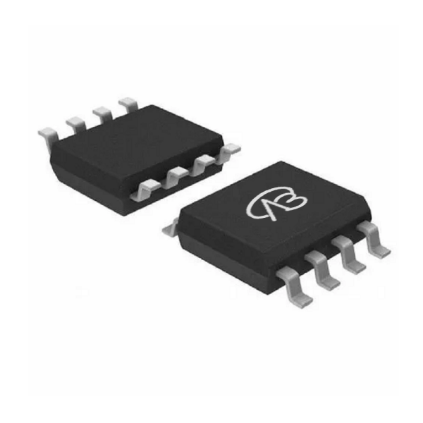
Product parameter:
| VB Package |
Configuration |
VDS(V) |
VGS |
Vthyp(V) |
ID(A) |
Rds2.5 |
Rds4.5 |
Rds10 |
Technology |
| SOP8 |
Dual-N+N |
30V |
|
1.7V |
6.8/6.0A |
|
|
22mΩ |
Trench |
| VB Package |
Configuration |
VCE |
VGE |
VGEth(V) |
VCEsat15V |
ICE |
Technology |
| SOP8 |
Dual-N+N |
|
|
|
|
|
Trench |
| VB Package |
Configuration |
VDS(V) |
VGS |
Vthyp(V) |
ID(A) |
Rds18 |
Technology |
| SOP8 |
Dual-N+N |
30V |
|
1.7V |
6.8/6.0A |
|
Trench |
| VB Package |
Configuration |
VDS(V) |
VGS |
Vthyp(V) |
ID(A) |
Rds6 |
Technology |
| SOP8 |
Dual-N+N |
30V |
|
1.7V |
6.8/6.0A |
|
Trench |
| VB Package |
Polarity |
Vz / VR |
Pd |
VF |
IF |
IR |
Cd |
Type |
| SOP8 |
Dual-N+N |
|
|
|
|
|
|
|
Detailed parameter description
1. **Package**: SOP8
- The SOP8 package is suitable for surface mount technology, which helps to achieve high-density circuit board design and improves the thermal management performance of the device.
2. **Configuration**: Dual-channel N-channel
- This configuration includes two independent N-channel MOSFETs, which can handle two different loads or control loops at the same time, suitable for multi-function applications.
3. **Drain-source voltage (VDS)**: 30V
- The maximum drain-source voltage is 30V, which is suitable for stable operation in low-voltage switching applications.
4. **Gate-source voltage (VGS)**: ±20V
- The maximum gate-source voltage is ±20V, which provides sufficient gate drive voltage range to ensure stable operation of the MOSFET under various operating conditions.
5. **Threshold voltage (Vth)**: 1.7V
- The threshold voltage is 1.7V, which is suitable for low voltage drive applications.
6. **On-resistance (RDS(ON))**:
- 26mΩ at VGS = 4.5V
- 22mΩ at VGS = 10V
- Lower on-resistance reduces power consumption and improves circuit efficiency.
7. **Continuous drain current (ID)**: 6.8A / 6.0A
- The maximum continuous drain current is 6.8A and 6.0A respectively, which is suitable for handling medium power loads.
8. **Technology**: Trench
- Adopts Trench technology, which improves the device's conduction performance and switching speed, enhancing its application effect in efficient energy management.
Domain and module applications:
Application Examples
1. **Power Management**
- FDS8984-NL-VB is commonly used in low-voltage power management circuits. Its low on-resistance and fast switching speed make it suitable for applications such as DC-DC converters, regulators, and power distribution modules, helping to improve the overall efficiency and reliability of the system.
2. **Load Switch**
- In load switch applications, FDS8984-NL-VB can effectively control different types of power loads and is widely used in portable devices such as laptops and tablets to ensure stable operation and battery life of the device.
3. **Battery Protection Circuit**
- Due to its dual-channel configuration and low on-resistance, FDS8984-NL-VB is suitable for protection circuits in battery management systems to prevent battery overcharge, over-discharge or short circuit, extend battery life and ensure device safety.
4. **Motor drive**
- FDS8984-NL-VB can be used to drive small motors, especially in applications that require precise control and fast response, such as home appliances, automation equipment, and robotic systems, to ensure stable operation and fast response of the motor.
5. **High-efficiency switching circuit**
- In applications that require efficient switching operations, such as audio amplifiers and signal processing modules, the high switching speed and low power consumption characteristics of FDS8984-NL-VB make it an ideal choice, which can effectively reduce signal delays and energy loss.
FDS8984-NL-VB's dual-channel configuration, low on-resistance, and Trench technology make it widely used in low-voltage switching, power management, battery protection, and other fields, and is an ideal MOSFET choice in various electronic devices.
* Please note: the above is only an example application scenario, the specific application depends on the requirements and conditions of the system design. When using this device, consult its data sheet for detailed technical specifications and features
Technical support:
* If you have any questions about the product, please fill out the form to submit, we will reply you within 24 hours


 Download now

 中文
中文 English
 Back to previous page