 中文
中文 English
FDD6796A-VB Product details
 Back to previous page
Product introduction:
FDD6796A-VB MOSFET Product Introduction
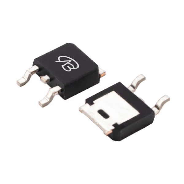
FDD6796A-VB is a single N-channel MOSFET designed for low voltage, high current applications, packaged in TO252. Its drain-source voltage (VDS) is 20V, and its gate-source voltage (VGS) withstand voltage is ±20V, which is suitable for low voltage and high current switching applications. The threshold voltage (Vth) range of this device is 0.5V to 1.5V, which can achieve effective conduction at a lower gate voltage. When VGS is 2.5V, the on-resistance (RDS(ON)) is 6mΩ, and when VGS is 4.5V, RDS(ON) is further reduced to 4.5mΩ. Its maximum continuous drain current (ID) is up to 100A. Based on advanced trench technology, it has extremely low switching losses and high efficiency, and is widely used in various high-efficiency power electronics applications.
FDD6796A-VB is a single N-channel MOSFET designed for low voltage, high current applications, packaged in TO252. Its drain-source voltage (VDS) is 20V, and its gate-source voltage (VGS) withstand voltage is ±20V, which is suitable for low voltage and high current switching applications. The threshold voltage (Vth) range of this device is 0.5V to 1.5V, which can achieve effective conduction at a lower gate voltage. When VGS is 2.5V, the on-resistance (RDS(ON)) is 6mΩ, and when VGS is 4.5V, RDS(ON) is further reduced to 4.5mΩ. Its maximum continuous drain current (ID) is up to 100A. Based on advanced trench technology, it has extremely low switching losses and high efficiency, and is widely used in various high-efficiency power electronics applications.
File download

Download PDF document
 Download now
Product parameter:
| VB Package | Configuration | VDS(V) | VGS | Vthyp(V) | ID(A) | Rds2.5 | Rds4.5 | Rds10 | Technology |
|---|---|---|---|---|---|---|---|---|---|
| TO252 | Single-N | 20V | 0.5~1.5V | 100A | 6mΩ | Trench |
| VB Package | Configuration | VCE | VGE | VGEth(V) | VCEsat15V | ICE | Technology |
|---|---|---|---|---|---|---|---|
| TO252 | Single-N | Trench |
| VB Package | Configuration | VDS(V) | VGS | Vthyp(V) | ID(A) | Rds18 | Technology |
|---|---|---|---|---|---|---|---|
| TO252 | Single-N | 20V | 0.5~1.5V | 100A | Trench |
| VB Package | Configuration | VDS(V) | VGS | Vthyp(V) | ID(A) | Rds6 | Technology |
|---|---|---|---|---|---|---|---|
| TO252 | Single-N | 20V | 0.5~1.5V | 100A | Trench |
| VB Package | Polarity | Vz / VR | Pd | VF | IF | IR | Cd | Type |
|---|---|---|---|---|---|---|---|---|
| TO252 | Single-N |
FDD6796A-VB MOSFET Detailed parameter description
- **Package type**: TO252
- **Polarity**: Single N-channel
- **Drain-source voltage (VDS)**: 20V
- **Gate-source voltage (VGS)**: ±20V
- **Threshold voltage (Vth)**: 0.5V ~ 1.5V
- **On-resistance (RDS(ON))**:
- 6mΩ @ VGS = 2.5V
- 4.5mΩ @ VGS = 4.5V
- **Continuous drain current (ID)**: 100A
- **Technology**: Trench
- **Input capacitance (Ciss)**: Low
- **Output capacitance (Coss)**: Low
- **Reverse recovery time (trr)**: Short
- **Power dissipation**: Low conduction and switching losses
- **Operating temperature range**: -55°C to +175°C
- **Package type**: TO252
- **Polarity**: Single N-channel
- **Drain-source voltage (VDS)**: 20V
- **Gate-source voltage (VGS)**: ±20V
- **Threshold voltage (Vth)**: 0.5V ~ 1.5V
- **On-resistance (RDS(ON))**:
- 6mΩ @ VGS = 2.5V
- 4.5mΩ @ VGS = 4.5V
- **Continuous drain current (ID)**: 100A
- **Technology**: Trench
- **Input capacitance (Ciss)**: Low
- **Output capacitance (Coss)**: Low
- **Reverse recovery time (trr)**: Short
- **Power dissipation**: Low conduction and switching losses
- **Operating temperature range**: -55°C to +175°C
Domain and module applications:
Application fields and module examples of FDD6796A-VB
FDD6796A-VB MOSFET is suitable for a variety of low voltage, high current application scenarios. Due to its low on-resistance and efficient switching characteristics, it is particularly suitable for the following fields:
1. **Low voltage DC-DC converter**: In low voltage DC-DC converters, FDD6796A-VB can achieve efficient power conversion, especially suitable for scenarios requiring high current and low loss, such as power modules for mobile electronic products such as laptops, smartphones, and wearable devices.
2. **Load switch application**: Due to its low RDS(ON) and high current carrying capacity, FDD6796A-VB is an ideal choice for load switches, especially in applications with high current demand and low loss, such as server power management, hard disk drives, and other data center equipment power modules.
3. **Battery Management System (BMS)**: In the battery management system, FDD6796A-VB can be used to control the charge and discharge current to ensure the safety and efficient energy utilization of the battery, especially suitable for lithium-ion battery packs, power tools and energy storage equipment.
4. **High-efficiency LED driver**: In the high-efficiency LED driver, FDD6796A-VB can provide stable current and fast response capability, suitable for high-performance lighting systems such as automotive headlights, commercial lighting and outdoor lighting.
FDD6796A-VB MOSFET, with its low-voltage and high-efficiency conduction characteristics, shows excellent performance in applications requiring high power density and low switching losses, and is an ideal choice for modern power electronics design.
FDD6796A-VB MOSFET is suitable for a variety of low voltage, high current application scenarios. Due to its low on-resistance and efficient switching characteristics, it is particularly suitable for the following fields:
1. **Low voltage DC-DC converter**: In low voltage DC-DC converters, FDD6796A-VB can achieve efficient power conversion, especially suitable for scenarios requiring high current and low loss, such as power modules for mobile electronic products such as laptops, smartphones, and wearable devices.
2. **Load switch application**: Due to its low RDS(ON) and high current carrying capacity, FDD6796A-VB is an ideal choice for load switches, especially in applications with high current demand and low loss, such as server power management, hard disk drives, and other data center equipment power modules.
3. **Battery Management System (BMS)**: In the battery management system, FDD6796A-VB can be used to control the charge and discharge current to ensure the safety and efficient energy utilization of the battery, especially suitable for lithium-ion battery packs, power tools and energy storage equipment.
4. **High-efficiency LED driver**: In the high-efficiency LED driver, FDD6796A-VB can provide stable current and fast response capability, suitable for high-performance lighting systems such as automotive headlights, commercial lighting and outdoor lighting.
FDD6796A-VB MOSFET, with its low-voltage and high-efficiency conduction characteristics, shows excellent performance in applications requiring high power density and low switching losses, and is an ideal choice for modern power electronics design.
* Please note: the above is only an example application scenario, the specific application depends on the requirements and conditions of the system design. When using this device, consult its data sheet for detailed technical specifications and features
Technical support:
* If you have any questions about the product, please fill out the form to submit, we will reply you within 24 hours


