 中文
中文 English
FDD3N50NZ-VB Product details
 Back to previous page
Product introduction:
FDD3N50NZ-VB Product Introduction
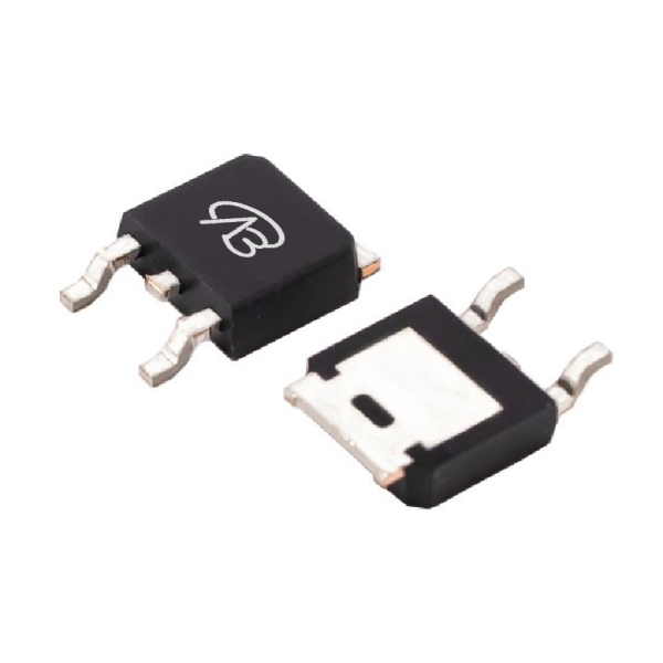
**FDD3N50NZ-VB** is a high voltage N-Channel MOSFET in TO252 package, designed for high voltage applications. Its maximum drain-to-source voltage (VDS) is 650V, which can work stably in high voltage environment. The threshold voltage (Vth) of this MOSFET is 3.5V, which ensures effective conduction under reasonable gate-source voltage. Its on-resistance (RDS(ON)) is 2750mΩ @ VGS=4.5V and 2200mΩ @ VGS=10V, which is relatively high, but it can still maintain good performance in high voltage applications. The maximum drain current (ID) of FDD3N50NZ-VB is 4A, which is suitable for applications with medium current requirements.
**Key Features:**
- **Package**: TO252
- **Configuration**: Single N-Channel
- **Maximum Drain-to-Source Voltage (VDS)**: 650V
- **Gate-Source Voltage (VGS)**: ±30V
- **Threshold Voltage (Vth)**: 3.5V
- **On-Resistance (RDS(ON))**: 2750mΩ @ VGS=4.5V; 2200mΩ @ VGS=10V
- **Maximum Drain Current (ID)**: 4A
- **Technology**: Plannar
**FDD3N50NZ-VB** is a high voltage N-Channel MOSFET in TO252 package, designed for high voltage applications. Its maximum drain-to-source voltage (VDS) is 650V, which can work stably in high voltage environment. The threshold voltage (Vth) of this MOSFET is 3.5V, which ensures effective conduction under reasonable gate-source voltage. Its on-resistance (RDS(ON)) is 2750mΩ @ VGS=4.5V and 2200mΩ @ VGS=10V, which is relatively high, but it can still maintain good performance in high voltage applications. The maximum drain current (ID) of FDD3N50NZ-VB is 4A, which is suitable for applications with medium current requirements.
**Key Features:**
- **Package**: TO252
- **Configuration**: Single N-Channel
- **Maximum Drain-to-Source Voltage (VDS)**: 650V
- **Gate-Source Voltage (VGS)**: ±30V
- **Threshold Voltage (Vth)**: 3.5V
- **On-Resistance (RDS(ON))**: 2750mΩ @ VGS=4.5V; 2200mΩ @ VGS=10V
- **Maximum Drain Current (ID)**: 4A
- **Technology**: Plannar
File download

Download PDF document
 Download now
Product parameter:
| VB Package | Configuration | VDS(V) | VGS | Vthyp(V) | ID(A) | Rds2.5 | Rds4.5 | Rds10 | Technology |
|---|---|---|---|---|---|---|---|---|---|
| TO252 | Single-N | 650V | 3.5V | 4A | 2200mΩ | Plannar |
| VB Package | Configuration | VCE | VGE | VGEth(V) | VCEsat15V | ICE | Technology |
|---|---|---|---|---|---|---|---|
| TO252 | Single-N | Plannar |
| VB Package | Configuration | VDS(V) | VGS | Vthyp(V) | ID(A) | Rds18 | Technology |
|---|---|---|---|---|---|---|---|
| TO252 | Single-N | 650V | 3.5V | 4A | Plannar |
| VB Package | Configuration | VDS(V) | VGS | Vthyp(V) | ID(A) | Rds6 | Technology |
|---|---|---|---|---|---|---|---|
| TO252 | Single-N | 650V | 3.5V | 4A | Plannar |
| VB Package | Polarity | Vz / VR | Pd | VF | IF | IR | Cd | Type |
|---|---|---|---|---|---|---|---|---|
| TO252 | Single-N |
Detailed parameter description
- **Package**: TO252
- Provides good heat dissipation performance and moderate size, suitable for medium power applications.
- **Configuration**: Single-N-Channel
- Suitable for application scenarios requiring a single N-Channel MOSFET, such as switching and amplifier circuits.
- **Maximum drain to source voltage (VDS)**: 650V
- High voltage tolerance, making it suitable for high voltage circuit design and power supply applications.
- **Gate-source voltage (VGS)**: ±30V
- Allows a wider gate-source voltage range, suitable for various control circuits.
- **Threshold voltage (Vth)**: 3.5V
- Can be effectively turned on at a reasonable gate-source voltage, suitable for medium and low voltage control applications.
- **On-resistance (RDS(ON))**:
- **2750mΩ @ VGS=4.5V**: At lower gate-source voltage, the on-resistance is higher, suitable for applications with lower current.
- **2200mΩ @ VGS=10V**: At higher gate-source voltage, the on-resistance decreases, suitable for high current applications.
- **Maximum drain current (ID)**: 4A
- Medium current carrying capability, suitable for switching and amplifying applications with medium current loads.
- **Technology**: Plannar
- Plannar technology provides higher voltage tolerance, but the on-resistance is relatively high, suitable for high voltage applications.
- **Package**: TO252
- Provides good heat dissipation performance and moderate size, suitable for medium power applications.
- **Configuration**: Single-N-Channel
- Suitable for application scenarios requiring a single N-Channel MOSFET, such as switching and amplifier circuits.
- **Maximum drain to source voltage (VDS)**: 650V
- High voltage tolerance, making it suitable for high voltage circuit design and power supply applications.
- **Gate-source voltage (VGS)**: ±30V
- Allows a wider gate-source voltage range, suitable for various control circuits.
- **Threshold voltage (Vth)**: 3.5V
- Can be effectively turned on at a reasonable gate-source voltage, suitable for medium and low voltage control applications.
- **On-resistance (RDS(ON))**:
- **2750mΩ @ VGS=4.5V**: At lower gate-source voltage, the on-resistance is higher, suitable for applications with lower current.
- **2200mΩ @ VGS=10V**: At higher gate-source voltage, the on-resistance decreases, suitable for high current applications.
- **Maximum drain current (ID)**: 4A
- Medium current carrying capability, suitable for switching and amplifying applications with medium current loads.
- **Technology**: Plannar
- Plannar technology provides higher voltage tolerance, but the on-resistance is relatively high, suitable for high voltage applications.
Domain and module applications:
Applications and module examples
1. **High Voltage Switches**:
FDD3N50NZ-VB is suitable for high voltage switch applications due to its high voltage tolerance. For example, as a high voltage power switch, it can stably switch in a high voltage environment to ensure the reliability and safety of the circuit.
2. **Power Management**:
In the power management circuit, this MOSFET can be used to regulate and protect the high voltage power supply to ensure the stable output of the power supply and prevent overvoltage or overcurrent.
3. **Inverters**:
In the inverter design, FDD3N50NZ-VB can be used as the main switching element to provide high voltage operation capability to ensure that the inverter can stably convert DC power to AC power.
4. **Motor Drivers**:
Despite its relatively low current carrying capacity, the FDD3N50NZ-VB can still be used for motor control under high voltage conditions in low-power motor drive applications to ensure stable motor operation.
5. **High Voltage Circuit Protection**:
This MOSFET can be used in protection devices in high-voltage circuits, such as overvoltage protection circuits, to ensure that the circuit can safely cut off the current under abnormal conditions and protect other components from damage.
1. **High Voltage Switches**:
FDD3N50NZ-VB is suitable for high voltage switch applications due to its high voltage tolerance. For example, as a high voltage power switch, it can stably switch in a high voltage environment to ensure the reliability and safety of the circuit.
2. **Power Management**:
In the power management circuit, this MOSFET can be used to regulate and protect the high voltage power supply to ensure the stable output of the power supply and prevent overvoltage or overcurrent.
3. **Inverters**:
In the inverter design, FDD3N50NZ-VB can be used as the main switching element to provide high voltage operation capability to ensure that the inverter can stably convert DC power to AC power.
4. **Motor Drivers**:
Despite its relatively low current carrying capacity, the FDD3N50NZ-VB can still be used for motor control under high voltage conditions in low-power motor drive applications to ensure stable motor operation.
5. **High Voltage Circuit Protection**:
This MOSFET can be used in protection devices in high-voltage circuits, such as overvoltage protection circuits, to ensure that the circuit can safely cut off the current under abnormal conditions and protect other components from damage.
* Please note: the above is only an example application scenario, the specific application depends on the requirements and conditions of the system design. When using this device, consult its data sheet for detailed technical specifications and features
Technical support:
* If you have any questions about the product, please fill out the form to submit, we will reply you within 24 hours


