 中文
中文 English
FCD4N60-VB Product details
 Back to previous page
Product introduction:
FCD4N60-VB MOSFET Product Introduction
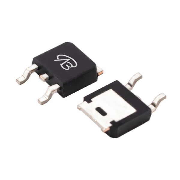
FCD4N60-VB is a high voltage N-channel MOSFET in TO252 package. It can withstand drain-source voltage up to 650V and maximum drain current of 5A. This MOSFET uses SJ_Multi-EPI technology, which is designed to provide low on-resistance and excellent high voltage tolerance. Despite its on-resistance of 1000mΩ, it can provide stable performance in high voltage applications and is suitable for various power management and switching applications that require high voltage support.
FCD4N60-VB is a high voltage N-channel MOSFET in TO252 package. It can withstand drain-source voltage up to 650V and maximum drain current of 5A. This MOSFET uses SJ_Multi-EPI technology, which is designed to provide low on-resistance and excellent high voltage tolerance. Despite its on-resistance of 1000mΩ, it can provide stable performance in high voltage applications and is suitable for various power management and switching applications that require high voltage support.
File download

Download PDF document
 Download now
Product parameter:
| VB Package | Configuration | VDS(V) | VGS | Vthyp(V) | ID(A) | Rds2.5 | Rds4.5 | Rds10 | Technology |
|---|---|---|---|---|---|---|---|---|---|
| TO252 | Single-N | 650V | 3.5V | 5A | 1000mΩ | SJ_Multi-EPI |
| VB Package | Configuration | VCE | VGE | VGEth(V) | VCEsat15V | ICE | Technology |
|---|---|---|---|---|---|---|---|
| TO252 | Single-N | SJ_Multi-EPI |
| VB Package | Configuration | VDS(V) | VGS | Vthyp(V) | ID(A) | Rds18 | Technology |
|---|---|---|---|---|---|---|---|
| TO252 | Single-N | 650V | 3.5V | 5A | SJ_Multi-EPI |
| VB Package | Configuration | VDS(V) | VGS | Vthyp(V) | ID(A) | Rds6 | Technology |
|---|---|---|---|---|---|---|---|
| TO252 | Single-N | 650V | 3.5V | 5A | SJ_Multi-EPI |
| VB Package | Polarity | Vz / VR | Pd | VF | IF | IR | Cd | Type |
|---|---|---|---|---|---|---|---|---|
| TO252 | Single-N |
FCD4N60-VB MOSFET Detailed parameter description
- **Package type**: TO252
- **Configuration**: Single N-channel
- **Maximum drain-source voltage (VDS)**: 650V
- **Gate-source voltage (VGS)**: ±30V
- **Threshold voltage (Vth)**: 3.5V
- **On-resistance (RDS(ON))**: 1000mΩ @ VGS=10V
- **Maximum continuous drain current (ID)**: 5A
- **Technology**: SJ_Multi-EPI
- **Package type**: TO252
- **Configuration**: Single N-channel
- **Maximum drain-source voltage (VDS)**: 650V
- **Gate-source voltage (VGS)**: ±30V
- **Threshold voltage (Vth)**: 3.5V
- **On-resistance (RDS(ON))**: 1000mΩ @ VGS=10V
- **Maximum continuous drain current (ID)**: 5A
- **Technology**: SJ_Multi-EPI
Domain and module applications:
Application fields and modules
The high voltage and moderate current characteristics of FCD4N60-VB make it suitable for the following fields and modules:
1. **High voltage switching circuit**:
- **Application scenario**: High voltage switching power supply, switch mode power supply
- **Description**: The 650V VDS of FCD4N60-VB makes it very suitable for high voltage switching circuits. In high voltage switching power supplies, MOSFET can withstand high voltage and maintain stable performance, suitable for power switches and protection circuits.
2. **Power management system**:
- **Application scenario**: Power converter, power regulation
- **Description**: In power management systems, FCD4N60-VB provides reliable power conversion and power regulation functions. It can handle high voltages and provide stable support for power regulation, suitable for high voltage power modules.
3. **Industrial drive circuits**:
- **Application scenarios**: High voltage motor drive, industrial power supply
- **Description**: FCD4N60-VB performs well in high voltage motor drive and industrial power supply applications. Its high voltage tolerance ensures stable operation when driving high voltage motors.
4. **Power electronic equipment**:
- **Application scenarios**: High voltage inverter, power amplifier
- **Description**: FCD4N60-VB is suitable for power electronic equipment such as high voltage inverters and power amplifiers. Its high voltage and moderate current characteristics enable it to provide stable and reliable performance in these high power applications.
5. **High Voltage Power Module**:
- **Application Scenario**: High Voltage DC Power Supply, High Voltage Power Conversion
- **Description**: In high voltage DC power supply and power conversion applications, the high voltage capability of FCD4N60-VB enables it to handle high power, high voltage power modules, providing effective power management and conversion.
The high voltage tolerance and moderate current handling capability of FCD4N60-VB enable it to perform well in high voltage and current applications, and is particularly suitable for power supplies and switching circuits that need to handle high voltages.
The high voltage and moderate current characteristics of FCD4N60-VB make it suitable for the following fields and modules:
1. **High voltage switching circuit**:
- **Application scenario**: High voltage switching power supply, switch mode power supply
- **Description**: The 650V VDS of FCD4N60-VB makes it very suitable for high voltage switching circuits. In high voltage switching power supplies, MOSFET can withstand high voltage and maintain stable performance, suitable for power switches and protection circuits.
2. **Power management system**:
- **Application scenario**: Power converter, power regulation
- **Description**: In power management systems, FCD4N60-VB provides reliable power conversion and power regulation functions. It can handle high voltages and provide stable support for power regulation, suitable for high voltage power modules.
3. **Industrial drive circuits**:
- **Application scenarios**: High voltage motor drive, industrial power supply
- **Description**: FCD4N60-VB performs well in high voltage motor drive and industrial power supply applications. Its high voltage tolerance ensures stable operation when driving high voltage motors.
4. **Power electronic equipment**:
- **Application scenarios**: High voltage inverter, power amplifier
- **Description**: FCD4N60-VB is suitable for power electronic equipment such as high voltage inverters and power amplifiers. Its high voltage and moderate current characteristics enable it to provide stable and reliable performance in these high power applications.
5. **High Voltage Power Module**:
- **Application Scenario**: High Voltage DC Power Supply, High Voltage Power Conversion
- **Description**: In high voltage DC power supply and power conversion applications, the high voltage capability of FCD4N60-VB enables it to handle high power, high voltage power modules, providing effective power management and conversion.
The high voltage tolerance and moderate current handling capability of FCD4N60-VB enable it to perform well in high voltage and current applications, and is particularly suitable for power supplies and switching circuits that need to handle high voltages.
* Please note: the above is only an example application scenario, the specific application depends on the requirements and conditions of the system design. When using this device, consult its data sheet for detailed technical specifications and features
Technical support:
* If you have any questions about the product, please fill out the form to submit, we will reply you within 24 hours


