 中文
中文 English
D4102L-VB Product details
 Back to previous page
Product introduction:
D4102L-VB MOSFET Product Introduction
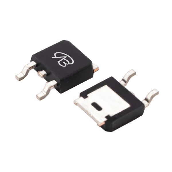
The D4102L-VB is a high-performance single N-channel MOSFET in TO252 package. It uses Trench technology to provide excellent on-resistance and high current capability. The maximum drain-source voltage (VDS) of this device is 30V, suitable for low-voltage switching applications. The operating range of the gate-source voltage (VGS) is ±20V, allowing a wide range of control voltage selection. The threshold voltage (Vth) of the D4102L-VB is 1.7V, enabling it to turn on at a lower gate voltage. Its on-resistance (RDS(ON)) is 9mΩ at VGS=4.5V and 7mΩ at VGS=10V, and the maximum drain current (ID) is 70A. Its low on-resistance and high current capability make it excel in high-efficiency applications.
The D4102L-VB is a high-performance single N-channel MOSFET in TO252 package. It uses Trench technology to provide excellent on-resistance and high current capability. The maximum drain-source voltage (VDS) of this device is 30V, suitable for low-voltage switching applications. The operating range of the gate-source voltage (VGS) is ±20V, allowing a wide range of control voltage selection. The threshold voltage (Vth) of the D4102L-VB is 1.7V, enabling it to turn on at a lower gate voltage. Its on-resistance (RDS(ON)) is 9mΩ at VGS=4.5V and 7mΩ at VGS=10V, and the maximum drain current (ID) is 70A. Its low on-resistance and high current capability make it excel in high-efficiency applications.
File download

Download PDF document
 Download now
Product parameter:
| VB Package | Configuration | VDS(V) | VGS | Vthyp(V) | ID(A) | Rds2.5 | Rds4.5 | Rds10 | Technology |
|---|---|---|---|---|---|---|---|---|---|
| TO252 | Single-N | 30V | 1.7V | 70A | 7mΩ | Trench |
| VB Package | Configuration | VCE | VGE | VGEth(V) | VCEsat15V | ICE | Technology |
|---|---|---|---|---|---|---|---|
| TO252 | Single-N | Trench |
| VB Package | Configuration | VDS(V) | VGS | Vthyp(V) | ID(A) | Rds18 | Technology |
|---|---|---|---|---|---|---|---|
| TO252 | Single-N | 30V | 1.7V | 70A | Trench |
| VB Package | Configuration | VDS(V) | VGS | Vthyp(V) | ID(A) | Rds6 | Technology |
|---|---|---|---|---|---|---|---|
| TO252 | Single-N | 30V | 1.7V | 70A | Trench |
| VB Package | Polarity | Vz / VR | Pd | VF | IF | IR | Cd | Type |
|---|---|---|---|---|---|---|---|---|
| TO252 | Single-N |
Detailed parameter description
| Parameter| Value| Unit|
|-------------------|------------------------------|--------------|
| Package type| TO252 | - |
| Configuration| Single N-channel| - |
| Drain-source voltage (VDS) | 30 | V |
| Gate-source voltage (VGS) | ±20 | V |
| Threshold voltage (Vth) | 1.7 | V |
| On-resistance (RDS(ON)) | 9mΩ @ VGS=4.5V | mΩ |
| | 7mΩ @ VGS=10V | mΩ |
| Drain current (ID) | 70 | A |
| Technology| Trench | - |
| Parameter| Value| Unit|
|-------------------|------------------------------|--------------|
| Package type| TO252 | - |
| Configuration| Single N-channel| - |
| Drain-source voltage (VDS) | 30 | V |
| Gate-source voltage (VGS) | ±20 | V |
| Threshold voltage (Vth) | 1.7 | V |
| On-resistance (RDS(ON)) | 9mΩ @ VGS=4.5V | mΩ |
| | 7mΩ @ VGS=10V | mΩ |
| Drain current (ID) | 70 | A |
| Technology| Trench | - |
Domain and module applications:
Applications and modules
The excellent performance of D4102L-VB makes it suitable for the following fields and modules:
1. **Power management**:
In power management systems, D4102L-VB can be used as an efficient switching element for DC-DC converters and regulators. Its low on-resistance and high current capability improve conversion efficiency and reduce power consumption, making it suitable for power supply designs that require high efficiency.
2. **Load switch**:
D4102L-VB is suitable for a variety of load switch applications, including load control in home appliances, automotive electronics, and industrial equipment. Its high current handling capability and low on-resistance ensure reliable control of the load and low power loss.
3. **Battery management system**:
In battery management systems, D4102L-VB can be used as a battery protection switch to handle high currents and ensure efficient operation of the system. Its excellent current handling capability and low on-resistance are suitable for high power requirements during battery charging and discharging.
4. **Power Amplifier**:
In power amplifier applications, the high current capability and low on-resistance of the D4102L-VB make it suitable as a load switch. It can effectively support the high current requirements of power amplifiers, thereby improving overall system performance.
5. **Inverters and Converters**:
In inverters and DC-DC converters, the D4102L-VB acts as a switching element that can handle high currents and maintain low on-resistance, thereby improving the efficiency of inverters and converters, especially in high-power application scenarios.
The low on-resistance and high current capability of the D4102L-VB make it an ideal choice for a variety of high-performance, high-current demand applications, including power management, load switching, battery protection, and power amplifiers.
The excellent performance of D4102L-VB makes it suitable for the following fields and modules:
1. **Power management**:
In power management systems, D4102L-VB can be used as an efficient switching element for DC-DC converters and regulators. Its low on-resistance and high current capability improve conversion efficiency and reduce power consumption, making it suitable for power supply designs that require high efficiency.
2. **Load switch**:
D4102L-VB is suitable for a variety of load switch applications, including load control in home appliances, automotive electronics, and industrial equipment. Its high current handling capability and low on-resistance ensure reliable control of the load and low power loss.
3. **Battery management system**:
In battery management systems, D4102L-VB can be used as a battery protection switch to handle high currents and ensure efficient operation of the system. Its excellent current handling capability and low on-resistance are suitable for high power requirements during battery charging and discharging.
4. **Power Amplifier**:
In power amplifier applications, the high current capability and low on-resistance of the D4102L-VB make it suitable as a load switch. It can effectively support the high current requirements of power amplifiers, thereby improving overall system performance.
5. **Inverters and Converters**:
In inverters and DC-DC converters, the D4102L-VB acts as a switching element that can handle high currents and maintain low on-resistance, thereby improving the efficiency of inverters and converters, especially in high-power application scenarios.
The low on-resistance and high current capability of the D4102L-VB make it an ideal choice for a variety of high-performance, high-current demand applications, including power management, load switching, battery protection, and power amplifiers.
* Please note: the above is only an example application scenario, the specific application depends on the requirements and conditions of the system design. When using this device, consult its data sheet for detailed technical specifications and features
Technical support:
* If you have any questions about the product, please fill out the form to submit, we will reply you within 24 hours


