 中文
中文 English
VBTA3230NS Product details
 Back to previous page
Product introduction:
VBTA3230NS 為雙 N+N 型 MOSFET,漏源電壓 (VDS) 為 20V,柵源電壓 (VGS) 為 20V,閾值電壓 (Vth) 為 0.5~1.5V,導通電阻 (RDS(on)) 為 350mΩ (VGS =2.5V),導通電阻 (RDS(on)) 為 300mΩ (VGS=4.5V),漏極電流 (ID) 為 0.6A。採用 Trench 工藝製造,封裝為 SC75-6。
File download

Download PDF document
 Download now
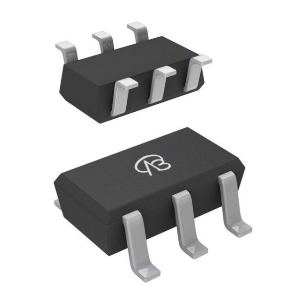
Product parameter:
| VB Package | Configuration | VDS(V) | VGS | Vthyp(V) | ID(A) | Rds2.5 | Rds4.5 | Rds10 | Technology |
|---|---|---|---|---|---|---|---|---|---|
| SC75-6 | Dual-N+N | 20V | 20(±V) | 0.5~1.5V | 0.6A | 350(mΩ) | 300(mΩ) | Trench |
參數: - 雙N+N型 - VDS(V): 20 - VGS(㊣V): 20 - Vth(V): 0.5~1.5 - RDS(on) VGS=2.5V(m次): 350 - RDS(on) VGS=4.5V(m次): 300 - ID (A): 0.6 - 技術:溝槽封裝:SC75-6
Domain and module applications:
由於其小封裝和低漏電流特性,VBTA3230NS 適用於輕載、低功耗的應用場景。例如,在移動設備中,可用於電池管理模組中的電源開關;在感測器電路中,可用作感測器信號調理電路中的開關管;在可攜式電子產品中,可用於充電管理模組中的電池充放電控制。其小封裝和低功耗使其在空間和能耗有限的場景中具有廣闊的應用潛力。
* Please note: the above is only an example application scenario, the specific application depends on the requirements and conditions of the system design. When using this device, consult its data sheet for detailed technical specifications and features
Technical support:
* If you have any questions about the product, please fill out the form to submit, we will reply you within 24 hours


