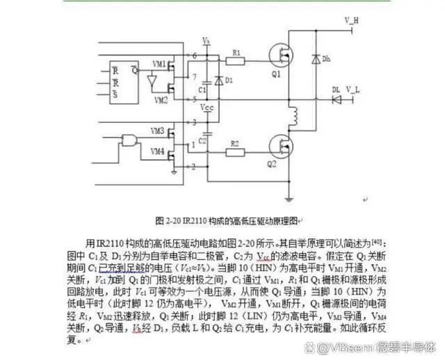
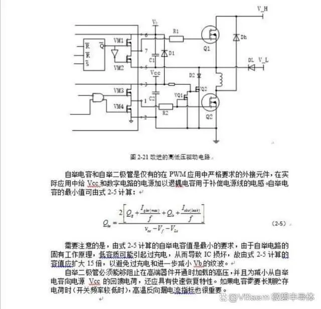
Regarding the practical application of MOSFETs using the IR2110 bootstrap driver, the circuit diagram and related explanatory text are as follows. The goal is to input two signals at the input of the IR2110, and when outputting the signal, the upper signal needs to be bootstrapped, while the lower signal does not require bootstrapping. VH in the picture is equal to 15V, VL is equal to 5V, and the MOSFET's turn-on voltage in the picture is 4.5V.


So, the questions for this issue are:
How much voltage do the two input signals need?
How large should Vb and Vcc be in the picture?
IR2110 is a high and low side driver that can be used to drive power devices such as MOSFETs or IGBTs. The bootstrap circuit in the IR2110 can provide the required power supply for the high side driver, enabling the normal operation of the high side driver. Specifically, the bootstrap circuit of the IR2110 can reverse the output signal of the high side driver to a capacitor, and then transfer the charge of the capacitor to the VCC pin of the high side driver through a diode, thereby providing the power supply voltage required by the high side driver.
【Last Issue's Answers】
Answer to Question One: If VCC is 3.3V, you only need to replace it with a PMOS and implement a pull-up to switch it on at a low level. You can directly use an open-drain design for the IO.
Analysis: When using an NMOS, the transistor should be connected between the load and ground; otherwise, the VGS voltage may not meet the requirements for saturation conduction. The way you connected it will cause the voltage obtained on the load to partially offset VGS, resulting in insufficient VGS and naturally insufficient voltage. However, if the NMOS is connected between the load and ground, and the load shares a common ground with the system, obviously, this connection is ineffective, while the Bluetooth board clearly requires a common ground with the system. Therefore, the power supply control method can only use a PMOS driver.
Answer to Question Two: From the diagram, the MOSFET's damage may be due to overvoltage breakdown. You can try adding a 16V voltage regulator at the GS terminals, or adding a filter capacitor at the switch end.
*To request free samples, please complete and submit the following information.
Our team will review your application within 24 hours and arrange shipment upon approval. Thank you!