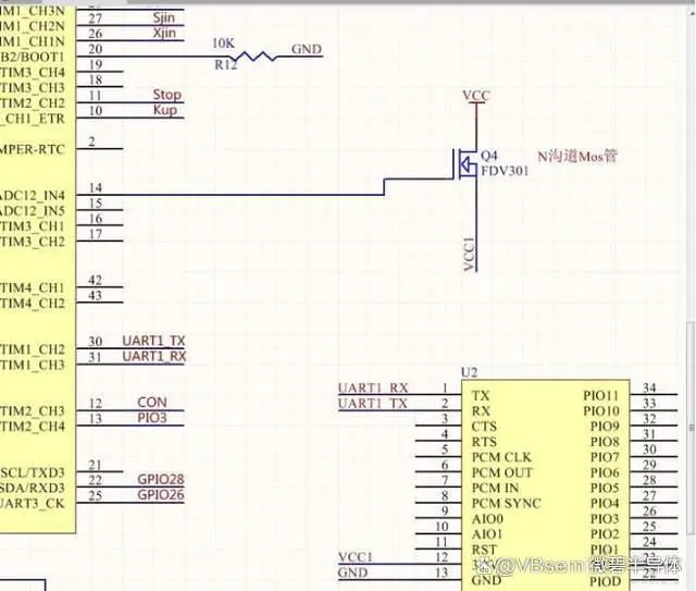
Why is the MOSFET voltage drop so large?

In the first scenario, a product design example requires low power consumption and uses an NMOS transistor, FDV301, to cut off power to Bluetooth during low power operation. However, it was found that when the MOSFET conducts, VCC is 3.3V while VCC1 is only 2.67V, making it impossible for Bluetooth to connect. What could be the reason for the large MOSFET voltage drop, and how should the circuit be modified?
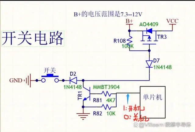
What causes MOSFETs to frequently burn out?

In the second scenario, a switch circuit using a P-MOSFET is powered by a battery with the microcontroller receiving power when the switch button is pressed, setting the IO port to 1 and providing a continuous low level to the MOSFET gate for startup. The issue here is the MOSFET frequently burns out. What could be the design problem causing this?
Note:
The gate-source voltage is normal when the gate is at 0V, with almost no voltage difference.
There were no abnormal phenomena during low-frequency switching tests.
【Last Issue's Answers】
Question 1: The STTH3010W fast recovery diode with If(av)=30A and Vrrm=1000V, in a DO-247 package, can be equipped with a large, low thermal resistance heatsink.
This should be sufficient. If not, reducing Vrrm to 600V allows for the selection of a power diode like the IDW100E60FKSA1, with a peak current of 400A and average forward current of 150A, in a TO-247 package, suitable for heatsink mounting, or even active cooling.
If this is still insufficient, consider selecting power devices like IGBTs, with ratings up to 270A, though their control circuits are more complex.
Question 2: The primary purpose of the LC low-pass filter at the front end is to filter out high-frequency components to prevent self-excitation and burning of the speaker, while also considering impedance matching. The description only mentions that it does not reduce the voltage stress on the MOSFETs, but it does not mention reducing the impact on the MOSFETs. Personally, I believe this RC circuit is used to suppress the impact current on the speaker load.
Furthermore, the main purpose of the LC low-pass filter at the front end is to filter out high-frequency components to prevent self-excitation and burning of the speaker. The source of high-frequency components is the high-frequency switching of the MOSFETs in the power amplifier chip's push-pull output, i.e., the high frequencies of the output PWM waveform. The LC filter certainly cannot filter out 100% of these, but it should attenuate them to a level that does not affect the speaker. Additionally, speakers are generally sensitive to both DC and high frequencies, so they are prone to self-excitation and burning under high-frequency interference.
Note: The RC circuit is used to suppress the impact current on the speaker load because the speaker has coils and magnets, acting as an inductor, so the speaker itself has a certain impact current. Therefore, some designs specifically add a freewheeling diode to the speaker.
*To request free samples, please complete and submit the following information.
Our team will review your application within 24 hours and arrange shipment upon approval. Thank you!