Recently, a low-power switch power supply was developed, and during the debugging process, it was found that the MOSFET was heating up severely. To solve the MOSFET heating problem, it is important to accurately determine the causes. Correct testing is crucial to identifying the problem. Through this experience, it was found that the key to solving the MOSFET heating problem lies in accurately selecting the test points and ensuring that the tests align with the analysis.
In the testing of switch power supplies, besides using a multimeter to measure the pin voltages of the control circuit and other components, it is important to use an oscilloscope to measure relevant voltage waveforms. When determining if the switch power supply is working properly, it is important to test areas that reflect the power supply's operational status, such as whether the primary and secondary windings of the transformer and the output feedback are reasonable, whether the switch MOSFET is working properly, whether the PWM controller output is normal (including the pulse amplitude and duty cycle), etc.
The rational selection of test points is crucial. Choosing test points that are both safe and reliable can quickly identify the cause of the fault.
The analysis of the cause of the MOSFET failure is based on previous knowledge of switch power supplies. Generally, the reasons for MOSFET heating are:
High drive frequency.
Insufficient gate drive voltage.
High Id current through the drain and source.
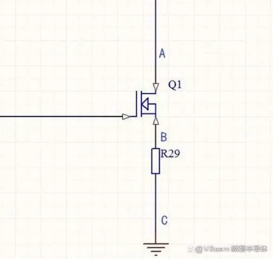
Therefore, the focus of the test should be on the MOSFET. Accurately testing its working condition is the fundamental issue. The selection of test points is as shown in the diagram:

Q1 is the power switch MOSFET, point A is the drain, point B is the source, R is the current sampling resistor, and point C is the ground terminal.
Connect the two probes of the dual-trace oscilloscope to points A and B, and simultaneously ground the two probe ground ends to the ground terminal C of the resistor R.

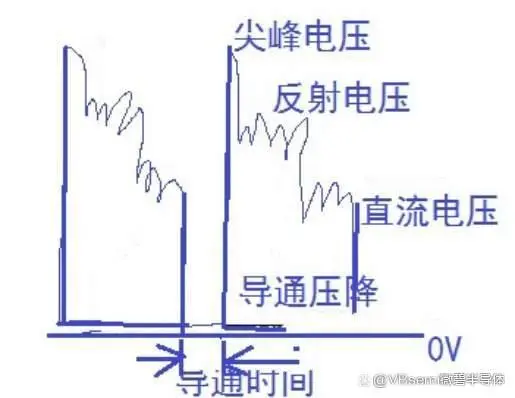
The waveform at point A of the MOSFET drain can be observed.
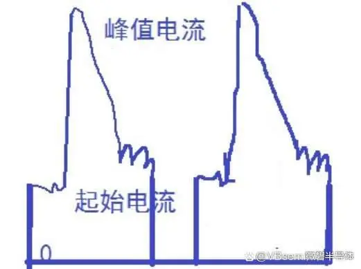
The waveform at point B indicates the source voltage of the MOSFET, which is the voltage waveform on the sampling resistor R and reflects information such as the drain current and the on and off times of the MOSFET, as analyzed below:
It can be seen that in each cycle, when the switch MOSFET conducts, the drain current rises from the start to the peak.

Points A and B are the two key test points, which basically reflect the working status and faults of the switch power supply. The peak voltage and current during conduction are very high. If the peak voltage and current during conduction can be eliminated, then the losses can be reduced by half, and the MOSFET heating problem can be solved. Of course, this is also the most direct reflection of whether the MOSFET is working properly.
After analyzing the test results, the gate drive resistor value was changed, and a suitable frequency was selected to create conditions for the MOSFET to be fully turned on. This effectively reduced the peak voltage. Additionally, a MOSFET with lower internal resistance was selected to reduce the voltage drop across the transistor during switching. A suitable heat sink was also chosen.
After these adjustments, the entire power supply was tested again. When the load was increased to full load, the MOSFET heating did not exceed 50°C, which was considered ideal.
During the oscilloscope testing process, special attention should be paid to the waveforms at these two test points. When gradually increasing the input voltage, if the peak voltage or current exceeds the design range and if there are any abnormal heating conditions of the MOSFET, the power supply should be immediately turned off to identify the cause and prevent MOSFET damage.
*To request free samples, please complete and submit the following information.
Our team will review your application within 24 hours and arrange shipment upon approval. Thank you!