I. Vehicle Power Supply
With the improvement of living standards, our requirements for cars have changed from simple means of transportation to multifunctional mobile places for entertainment, living, and work. Correspondingly, electronic devices such as laptops are indispensable. Electronic mobile devices generally use 220V/50Hz mains frequency AC power, while the 12V/24V DC power from the vehicle's battery cannot directly power our mobile electronic devices. Therefore, vehicle-mounted power converters, or inverters, have been developed. Compared with the commonly used modified sine wave inverters, pure sine wave inverters overcome the drawback of poor continuity of modified sine wave inverters and have the characteristics of strong safety, high power conversion efficiency, and simple control methods.
In 2020, Sun Jun Min designed a 500W power inverter with an input voltage of 20V DC and an output voltage of 220V/50Hz AC. According to experimental prototype testing, it has an efficiency of about 88% and features low noise and high reliability.

[Inverter circuit overall design diagram]
II. Overall Circuit
Main Parameters
DC-DC Boost Circuit + Control Circuit (Push-Pull Type):
Battery: VARTA 6-QW-6(580)-L
MOSFET: VD > 30V
Rectifier Diode: DSEI30
Main Control Chip: TL494
DC-AC Inverter Circuit + Control Circuit (Full Bridge Type):
MOSFET: VD = 600V, ID = 10A
Filter Capacitor: 2.25μf/2.4mH
Main Control Chip: TDS2285
20M Passive Crystal Oscillator
Rectifier: 1N4007
Magnetic Core: EE55
Optocoupler: TLP250
DC-DC Boost Circuit

[DC-DC Boost Main Circuit Diagram]
The DC-DC high-frequency boost section adopts a push-pull topology. In the DC-DC boost circuit, MOSFET is selected as the switching device. The maximum voltage that the field-effect transistor needs to withstand is about 30V. When selecting the MOSFET, the maximum withstand voltage of the MOSFET should have a margin. Here, you can choose VBsemi's NMOS VBM1606, VD=60V, ID=120A, with an extremely low on-state resistance Rds(on)=5mΩ.
Selectable MOSFET models:
VBM1606
VBL1615A
VBL1105
VBM1607V3
VBL1806

[Applicable VBsemi MOSFET Parameters]
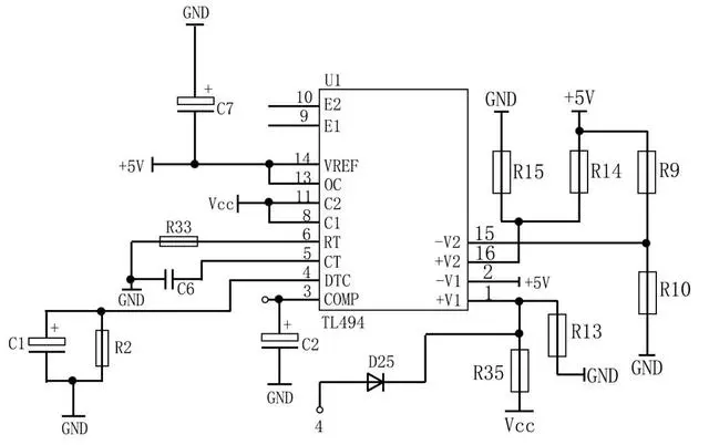
[DC-DC PWM Drive Circuit]
The DC-DC boost control circuit uses PWM pulse width modulation technology, with TL494 as the main control chip. It contains all the pulse width modulation control circuits internally, making it a chip that integrates all the modules required for switch power supply control.
DC-AC Inverter Circuit
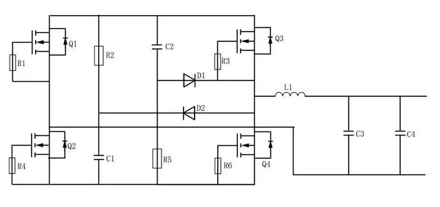
[DC-AC Inverter Circuit Schematic Diagram]
The main loop of the DC-AC inverter circuit adopts a full-bridge structure, and the diode parallel to the switch tube plays a protective role. The MOSFET can be selected as VBsemi's VBP16R20S, VD=600V, ID=20A, Rds(on)=190mΩ.
Selectable MOSFET models:
VBP16R20S
VBE16R10S
VBL16R11S
VBMB16R15S
VBM16036N
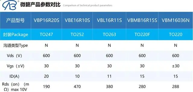
[Applicable VBsemi MOSFET Parameters]
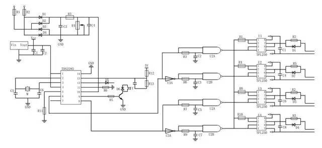
[DC-AC SPWM Drive Circuit]
The control circuit of the inverter section uses TDS2285 as the main control chip and uses the optocoupler chip TLP250 to increase the reliability of the hardware circuit.
Protection Circuit Design
To ensure the reliability of the power supply, its protection circuit consists of input reverse connection protection circuit, input overvoltage protection circuit, and undervoltage protection circuit.
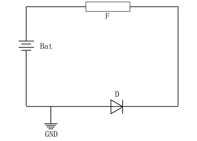
[Input Reverse Connection Protection Circuit]
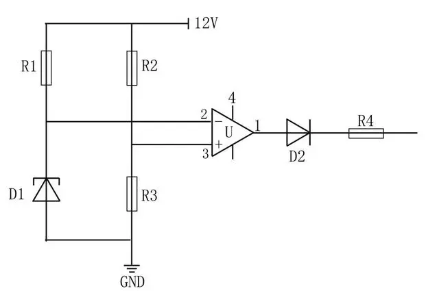
[Input Undervoltage Protection]
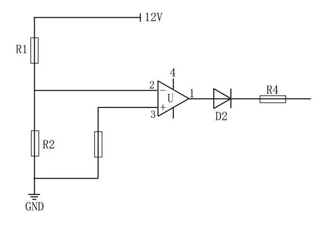
[Input Overvoltage Protection]
*To request free samples, please complete and submit the following information.
Our team will review your application within 24 hours and arrange shipment upon approval. Thank you!