We know that the MOS tube is a voltage-controlled device. Unlike bipolar transistors, the MOS tube conducts only when the voltage on the gate exceeds its threshold voltage, without requiring gate current. Therefore, fundamentally, no resistor is needed in series with the gate of the MOS tube.
For ordinary bipolar transistors, which are current-controlled devices, the base resistor is used to limit the base current. Otherwise, for the driving signal source, the base of the transistor becomes equivalent to a diode to ground, which affects the preceding driving circuit.
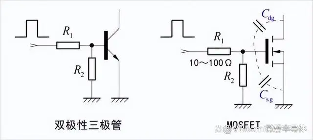
Since the gate of the MOS tube is insulated from the drain and source, no series resistor is needed on the gate for current limiting.
On the contrary, considering the parasitic capacitance on the gate of the MOS tube, to speed up the conduction and cut-off of the MOS tube, and reduce the loss during the conduction and cut-off processes, the equivalent resistance on its gate should be as small as possible.
However, in many practical MOS tube circuits, resistors are almost everywhere on the gate of the MOS tube. It seems that everyone has forgotten that the existence of this resistor will prolong the conduction and cut-off time of the MOS tube, increasing unnecessary losses.
So why is this resistor placed in front of the gate of the MOS tube in some circuits, and what is its function?
First, let's clarify a concept: analog circuits are not like software programming, where it's either 0 or 1. Instead, they are a continuous process of change. Both voltage on capacitors and current on inductors cannot change suddenly, otherwise catastrophic consequences will occur. Sharper rising and falling edges are not always better. Sometimes in design, even some resistors are intentionally added to make the rising and falling edges smoother to protect the components.
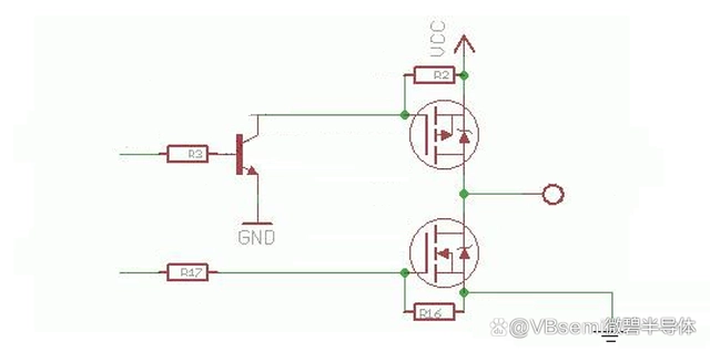
In the above circuit, resistor R17 serves three purposes: preventing oscillation, reducing the peak gate charging current, and protecting the MOS tube D-S junction from breakdown.
Firstly, in general, the I/O output port of the microcontroller will have some stray inductance. Under voltage sudden changes, it may form LC oscillation with the gate capacitance. When R17 is connected between them, it can increase damping and reduce the oscillation effect.
Secondly, when the gate voltage rises, the gate capacitance is charged first, and the charging peak current exceeds the output capability of the microcontroller's I/O. By connecting R17, the charging time can be slowed down, reducing the gate charging current.
Thirdly, when the gate is turned off, and the MOS tube's D-S junction changes from conduction to cut-off, the drain-source voltage VDS of the MOS tube will increase rapidly. If it is too large, the device will breakdown. Therefore, adding R17 can allow the gate capacitance to discharge slowly, preventing the device from breakdown.
So, how large should this resistor be?
This generally needs to be determined based on the actual situation. However, we can roughly judge the influence of the value by the following experiment.
In the following circuit, there is a resistor R3 in series with the gate of the MOS tube, and its drain-source load is an inductive load, including distributed line inductance.
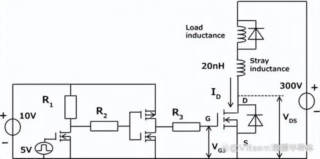
In the experiment, R3 was simulated with 1 ohm, 10 ohms, and 50 ohms, respectively. When R3 is 1 ohm, high-frequency oscillation signals can be seen on the output voltage Vds.

When R3 is increased to 10 ohms, the high-frequency oscillation signal on the output Vds is significantly attenuated.
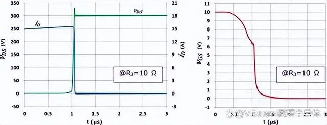
When R3 is increased to 50 ohms, the rising edge of Vds becomes relatively slow. A step caused by the Miller capacitance effect between the drain and gate also appears on its gate voltage. At this time, the power consumption of the corresponding MOS tube is greatly increased.
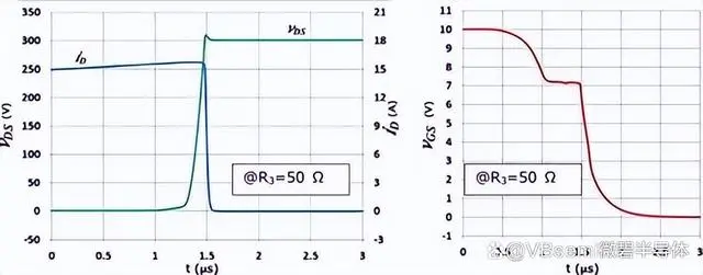
From the above experimental results, it can be seen that the resistor in series with the gate of the MOS tube needs to be determined according to the specific MOS tube and the distributed stray inductance of the circuit. If its value is too small, output ringing may occur; if it is too large, the switching transition time of the MOS tube will increase, thereby increasing power consumption.
*To request free samples, please complete and submit the following information.
Our team will review your application within 24 hours and arrange shipment upon approval. Thank you!