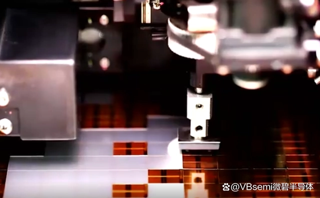
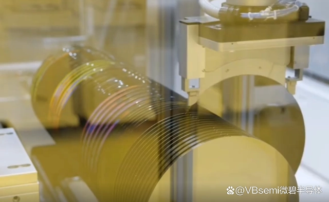
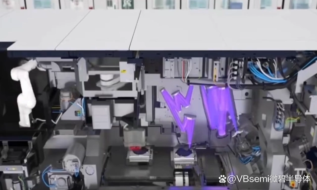
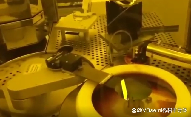
Semiconductor chips are manufactured through several processes, generally including the production of wafers, oxidation, photolithography, etching, thin film deposition, interconnection, testing, and packaging.

To obtain wafers, the first step is to prepare the materials for wafer production, with silicon being the most commonly used material. While silicon is abundant in nature, it requires refining due to impurities found in silicon sand. The refined silicon is melted and pulled into cylindrical ingots using the Czochralski process. These ingots are then sliced into thin wafers of a certain thickness, which serve as the raw material or "blank wafers."
The surfaces of these blank wafers are typically uneven and need to undergo processes such as grinding, chemical etching, polishing, and cleaning to remove surface imperfections and contaminants, resulting in clean and smooth surfaces.
After obtaining the wafers, the next step is oxidation. During this process, a protective oxide layer is formed on the wafer surface by exposing it to high temperatures in the presence of oxygen. This oxide layer serves to protect the wafer from impurities, prevent leakage currents, and facilitate subsequent processes.

Following oxidation is photolithography, which involves "printing" circuit patterns onto the wafer surface using light. This process includes applying a photoresist layer, exposing it to light through a photomask, and developing the pattern. The precision of these patterns is crucial for achieving high integration densities in the final chips and requires advanced photolithography techniques.
Etching is then used to remove any unwanted materials from the wafer surface while preserving the semiconductor circuit patterns created during photolithography. This process involves selectively removing materials using liquid, gas, or plasma etchants.
Thin film deposition is necessary for creating microdevices within the chip. This process involves depositing layers of thin films onto the wafer surface and selectively removing excess material through etching. Additional materials are also added to separate different devices.

Interconnection involves connecting the various components on the wafer surface to enable power and signal transmission. This is typically achieved using metal layers or multilayer interconnect structures.
Testing is performed to ensure the quality and reliability of the manufactured chips. Defective chips are identified and discarded, while those meeting quality standards proceed to the packaging stage.
Packaging involves several steps, including wafer dicing, die attachment, wire bonding, molding, and package testing. This process encapsulates the individual chips in protective packages and facilitates their connection to external circuits.
These are the basic steps involved in semiconductor chip manufacturing, although the actual process is much more complex and involves numerous additional steps and requirements.

*To request free samples, please complete and submit the following information.
Our team will review your application within 24 hours and arrange shipment upon approval. Thank you!